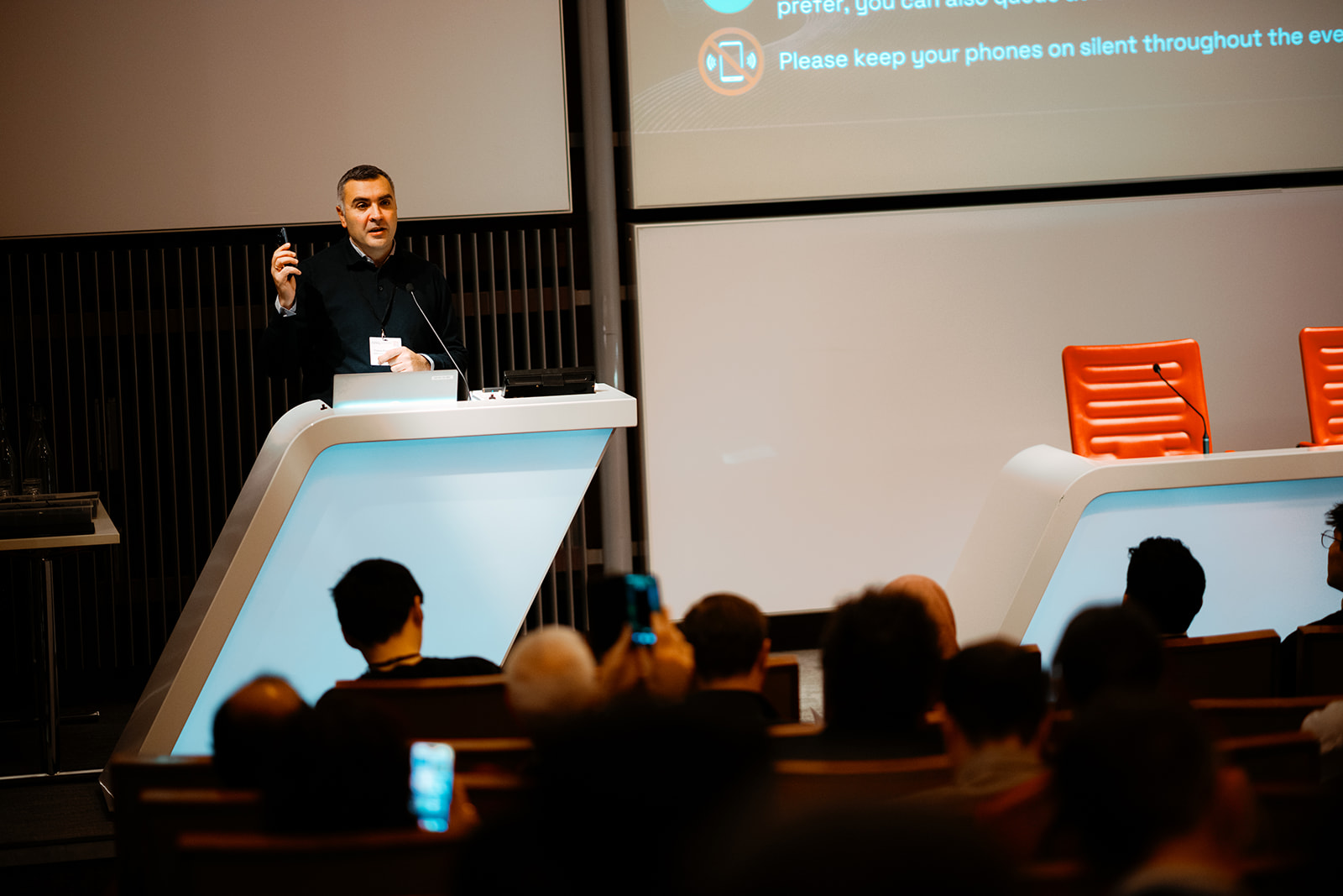
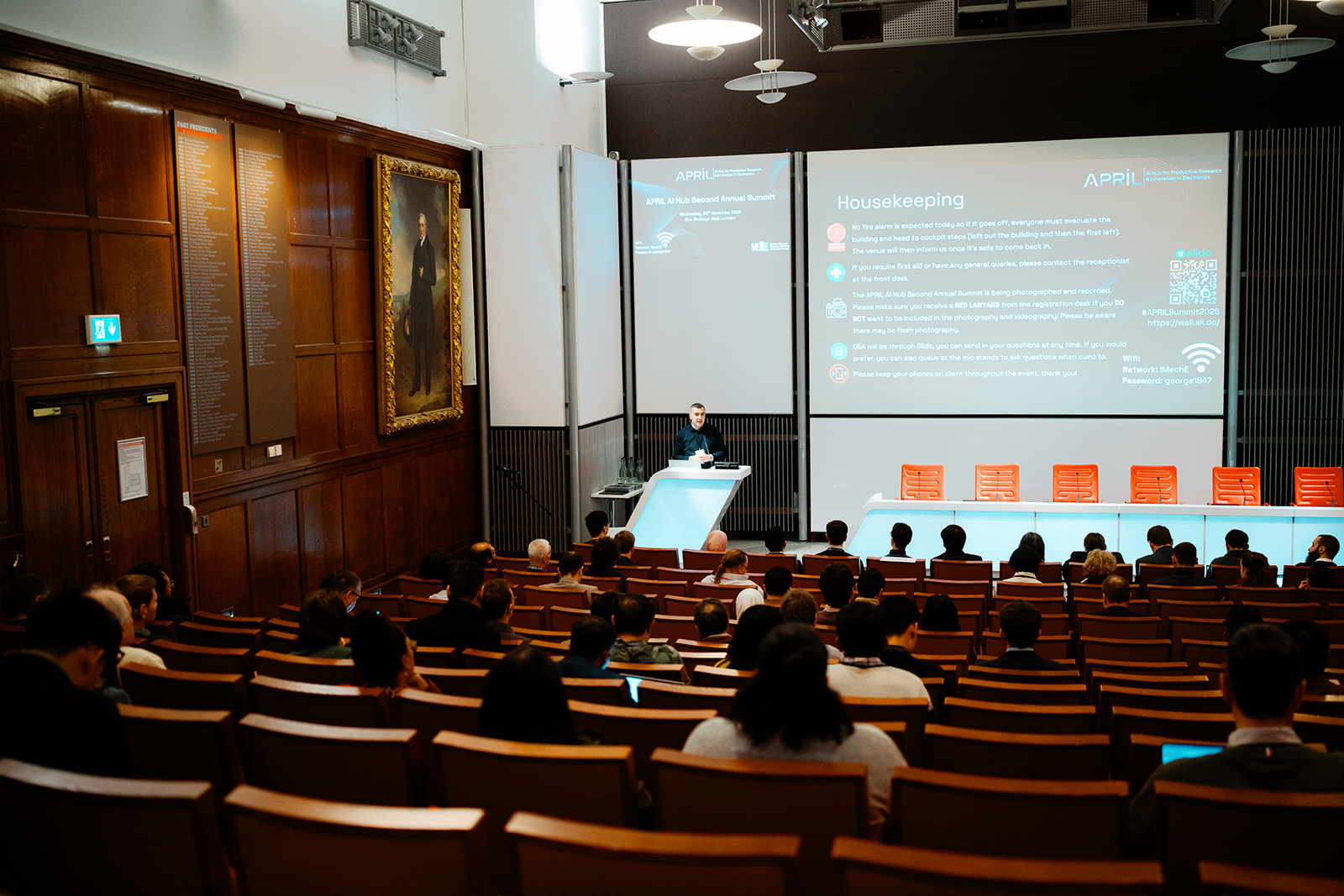
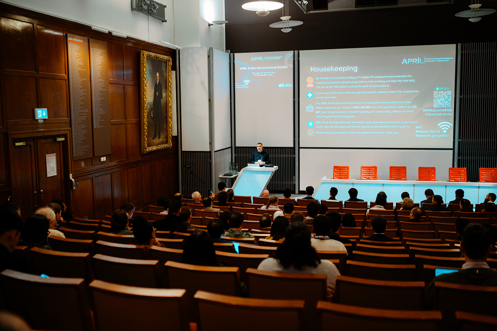
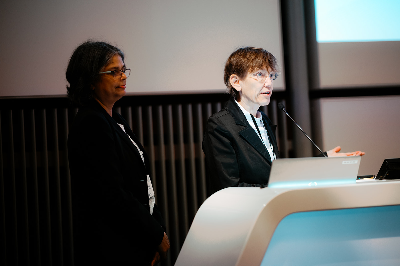
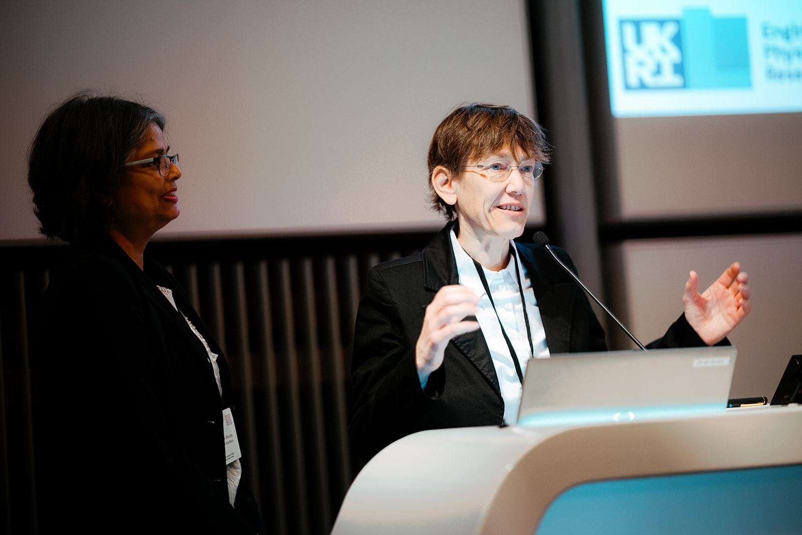
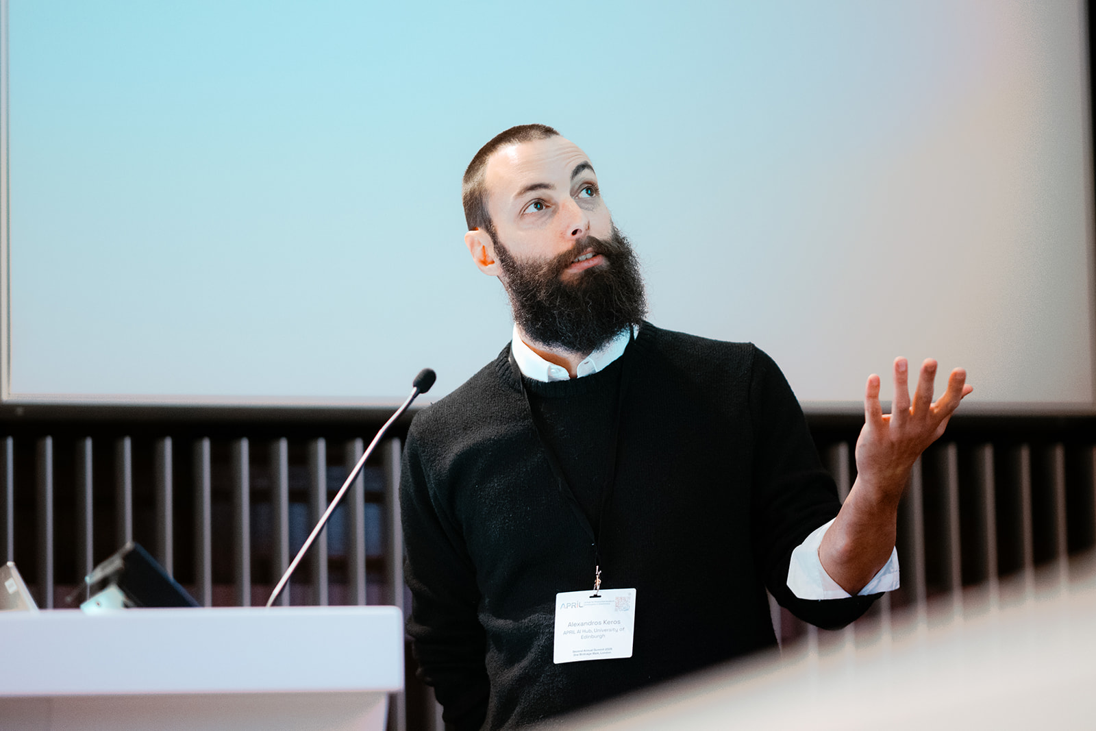
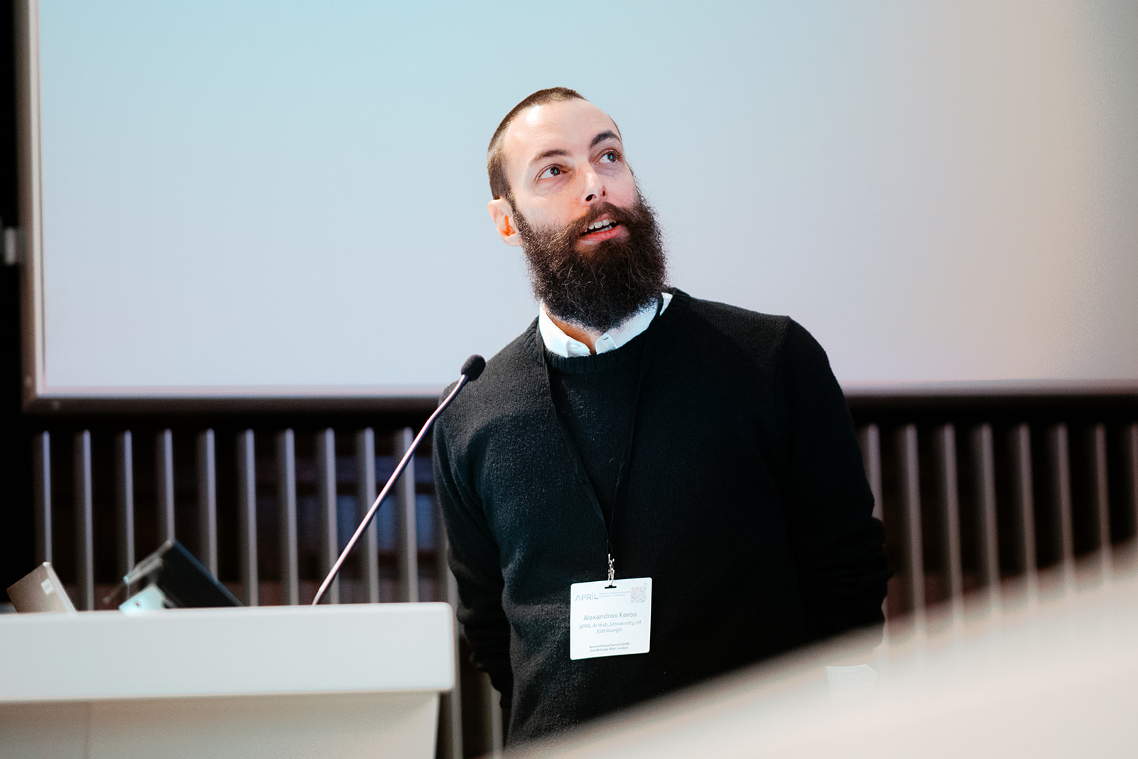
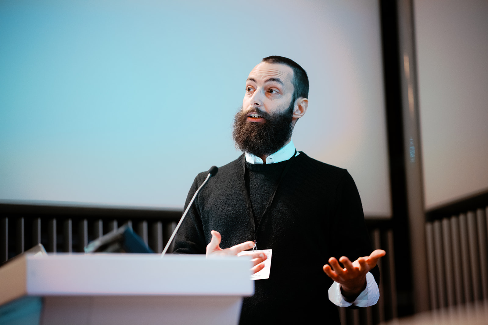
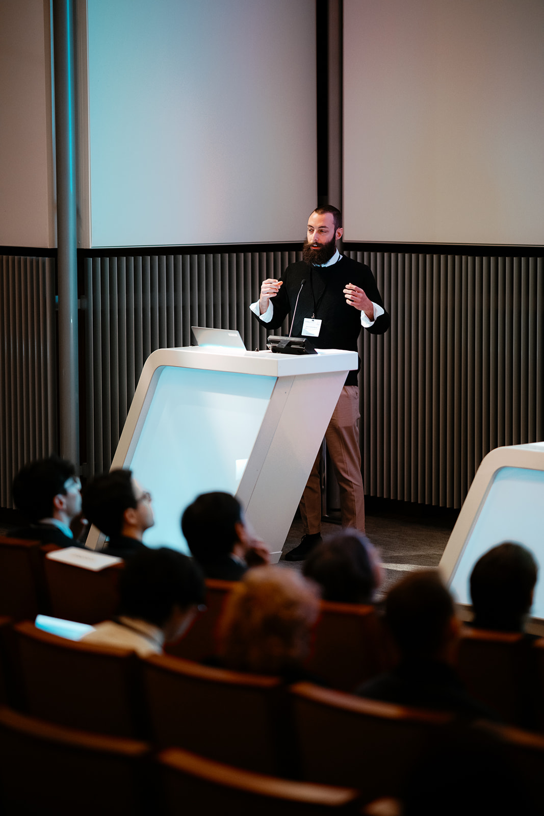
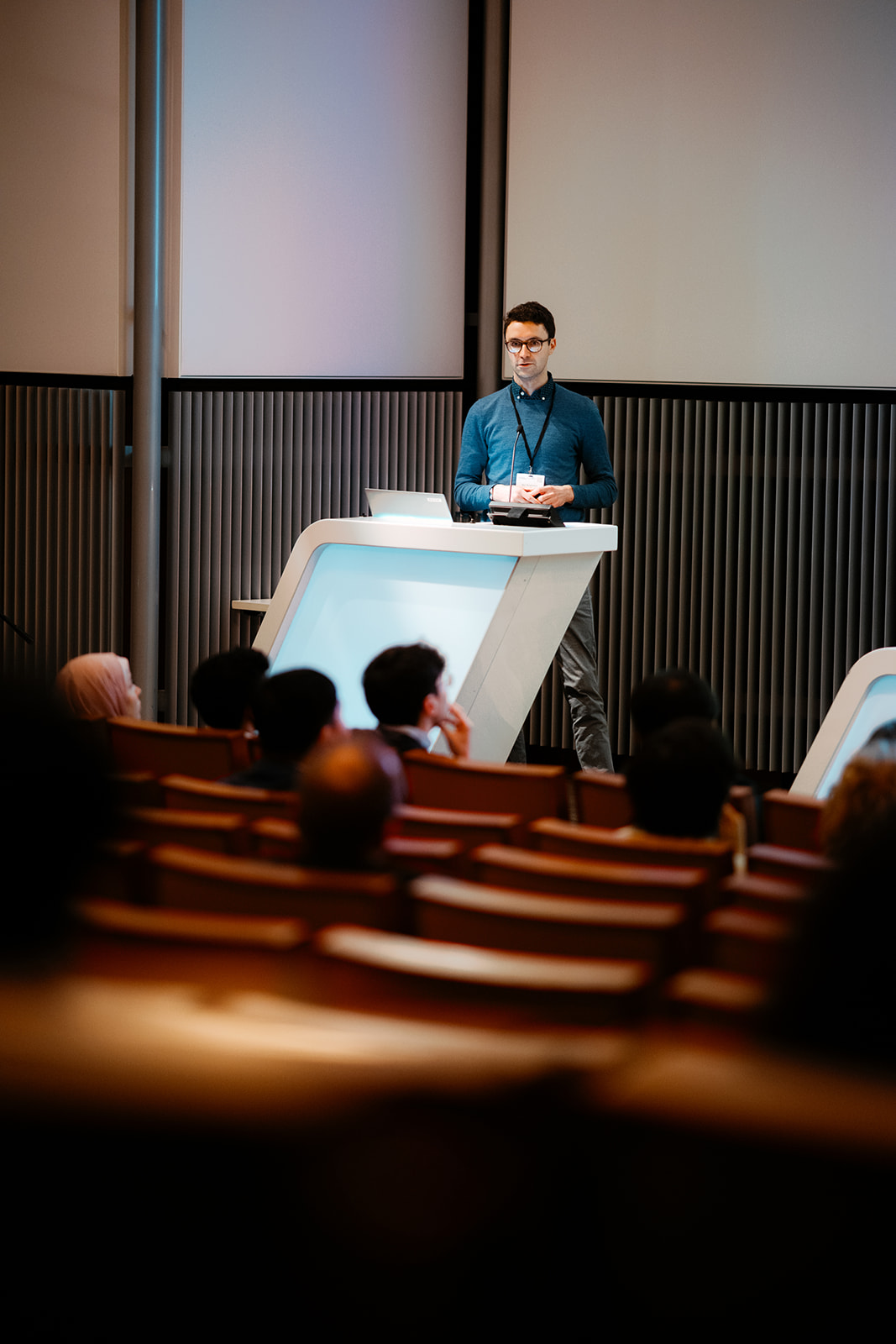
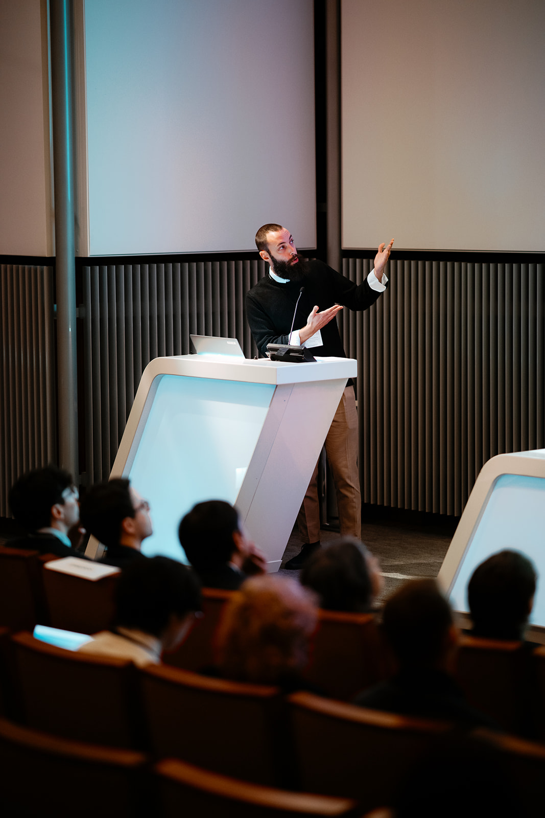
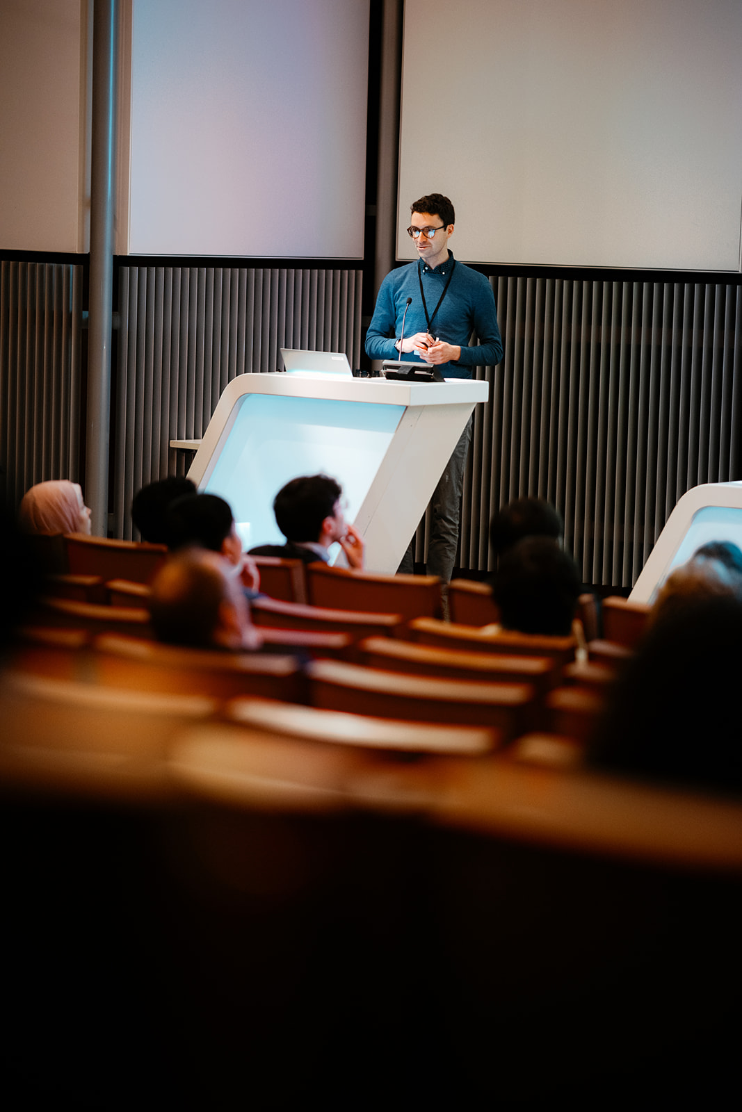
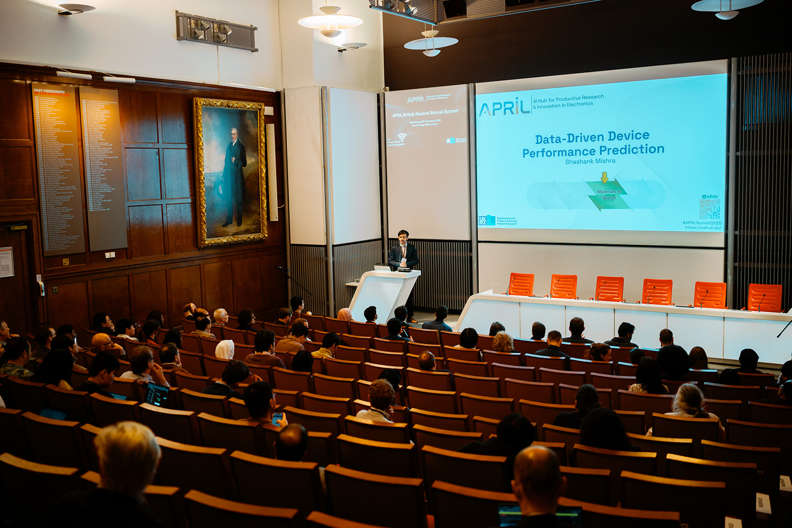
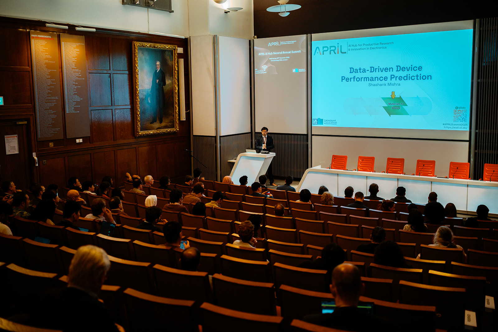
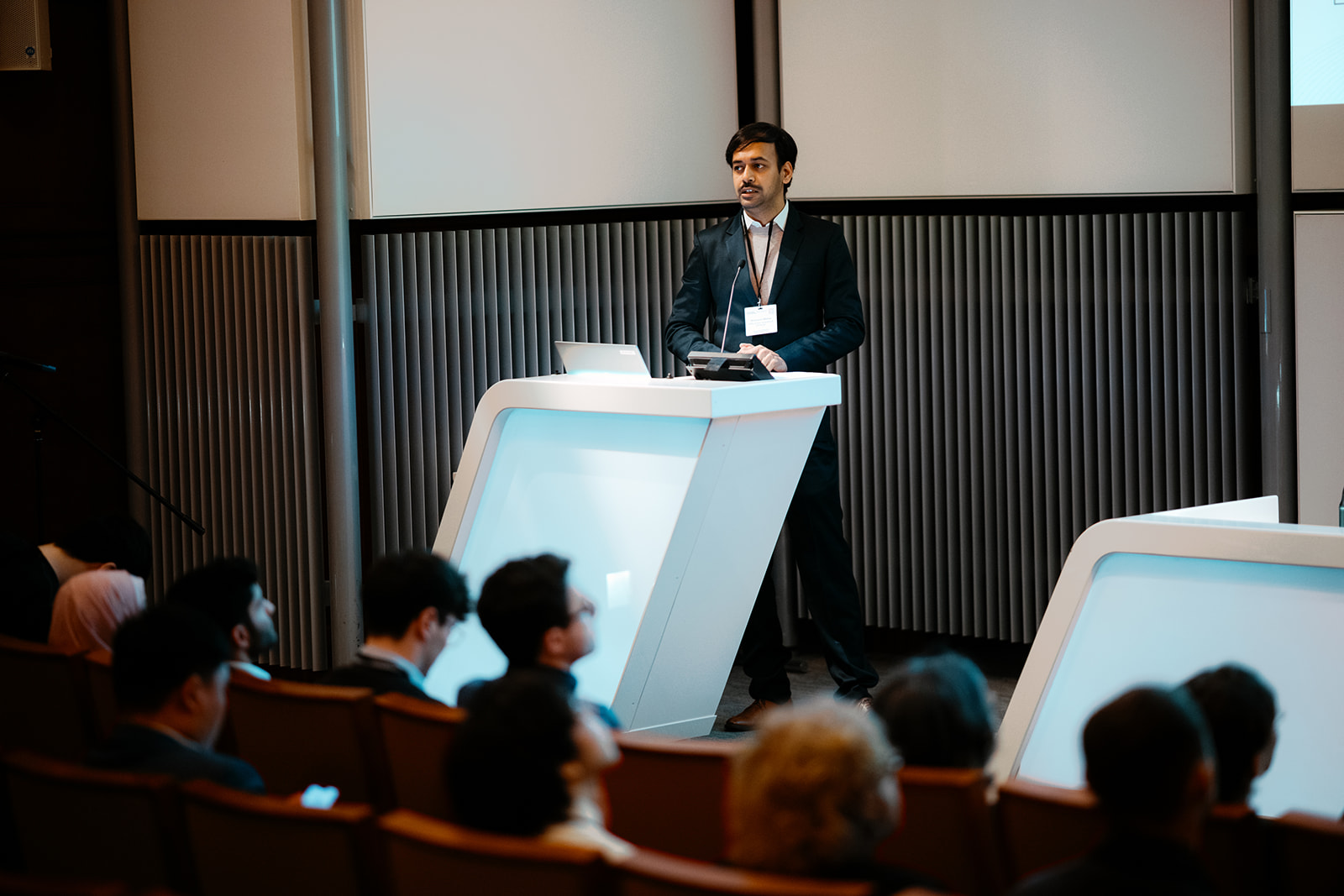
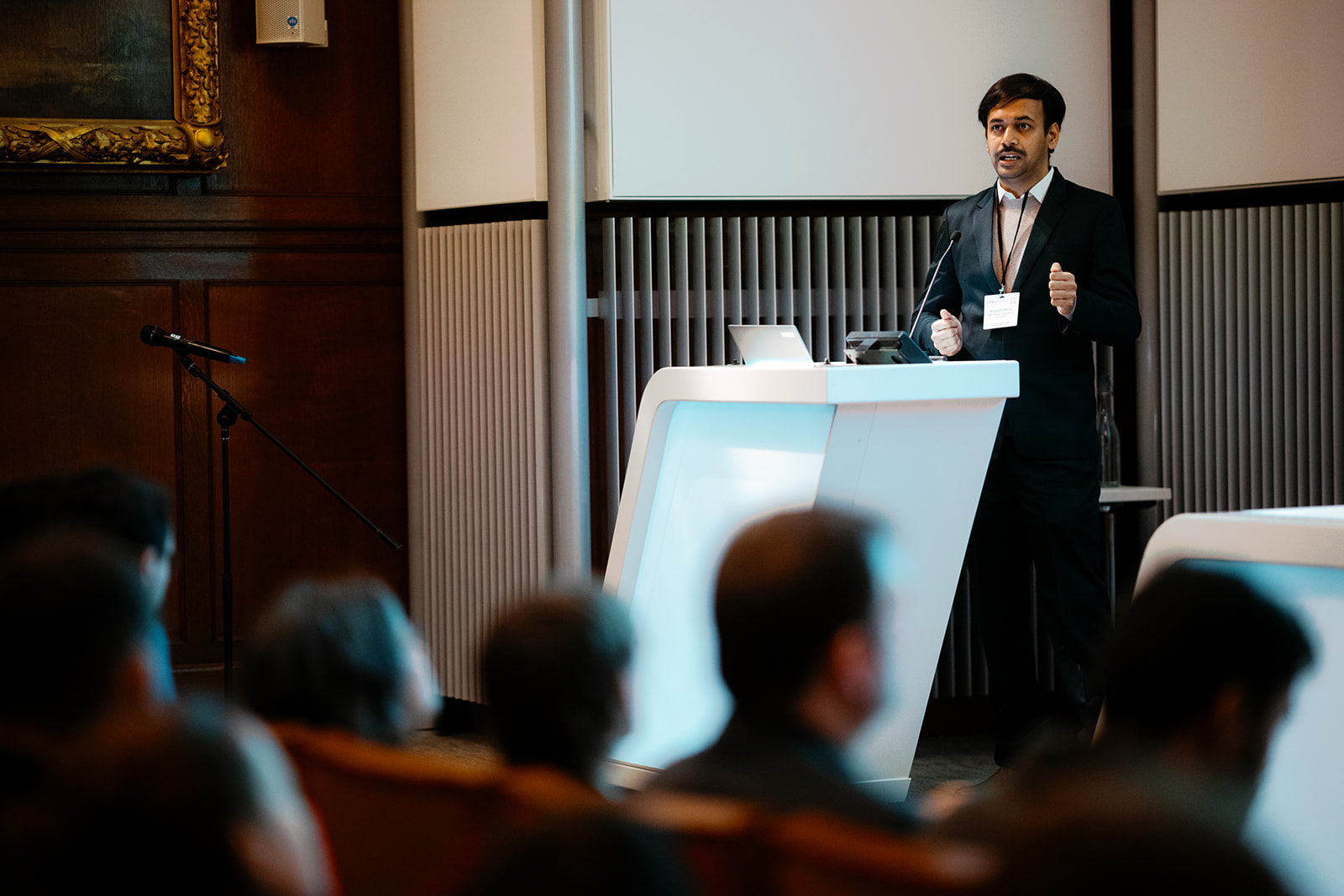
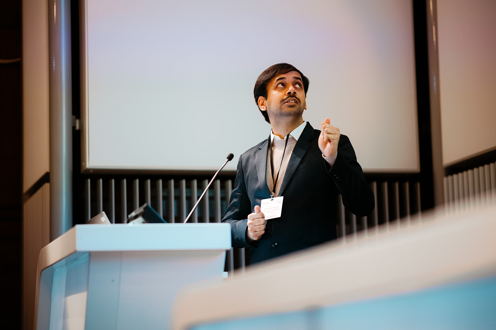
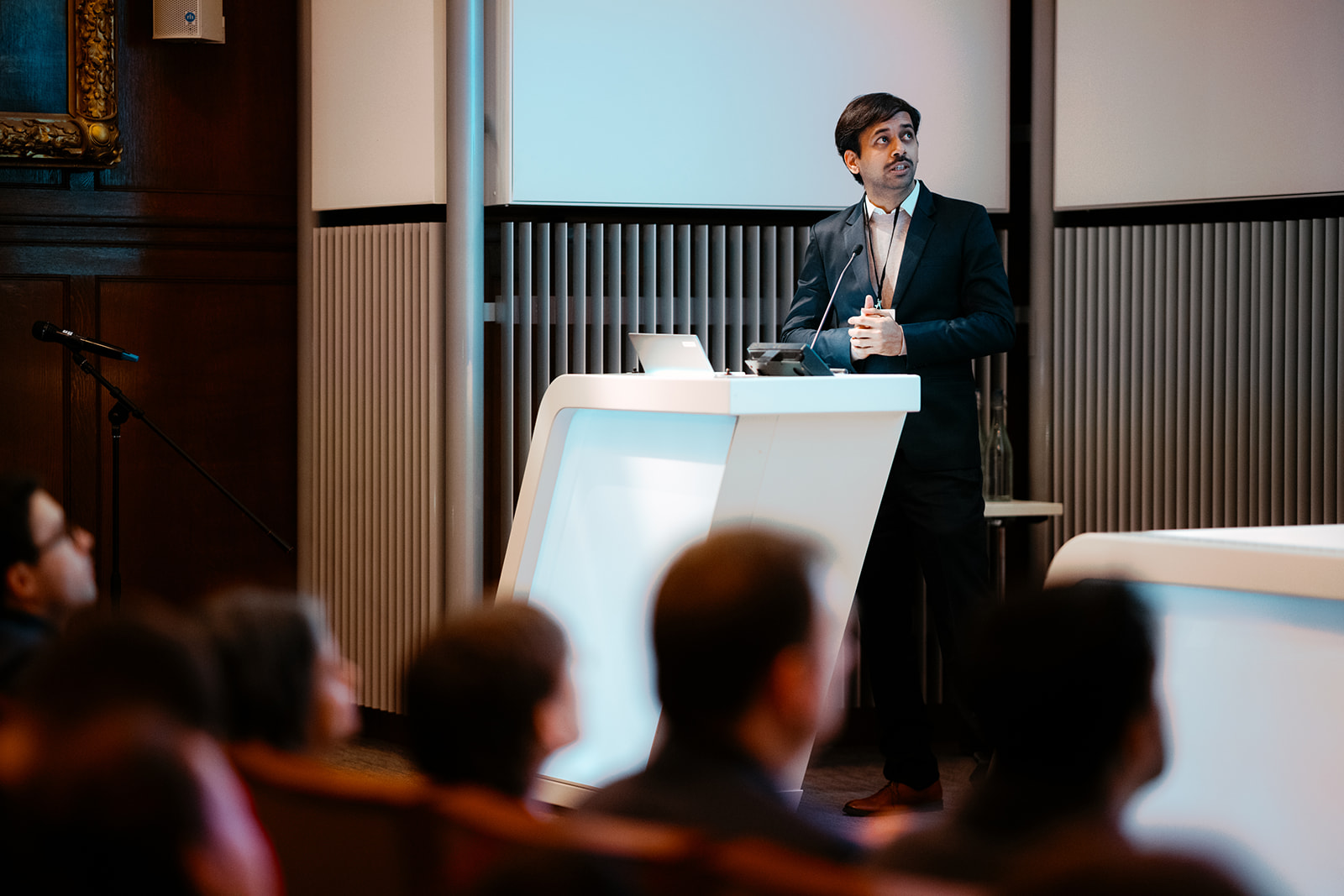
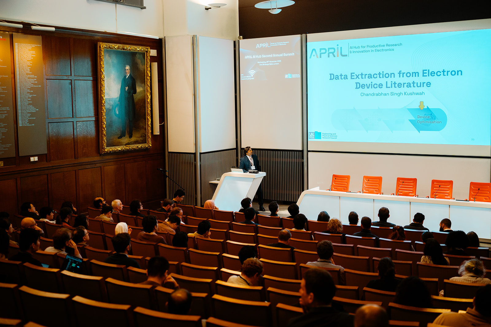
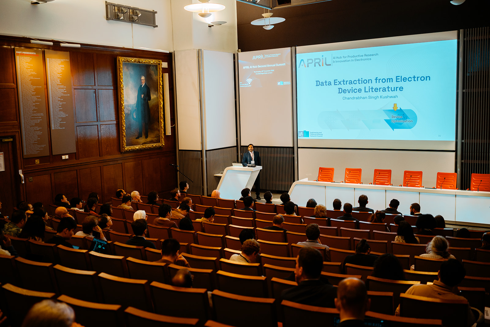
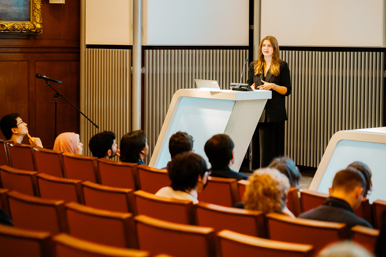
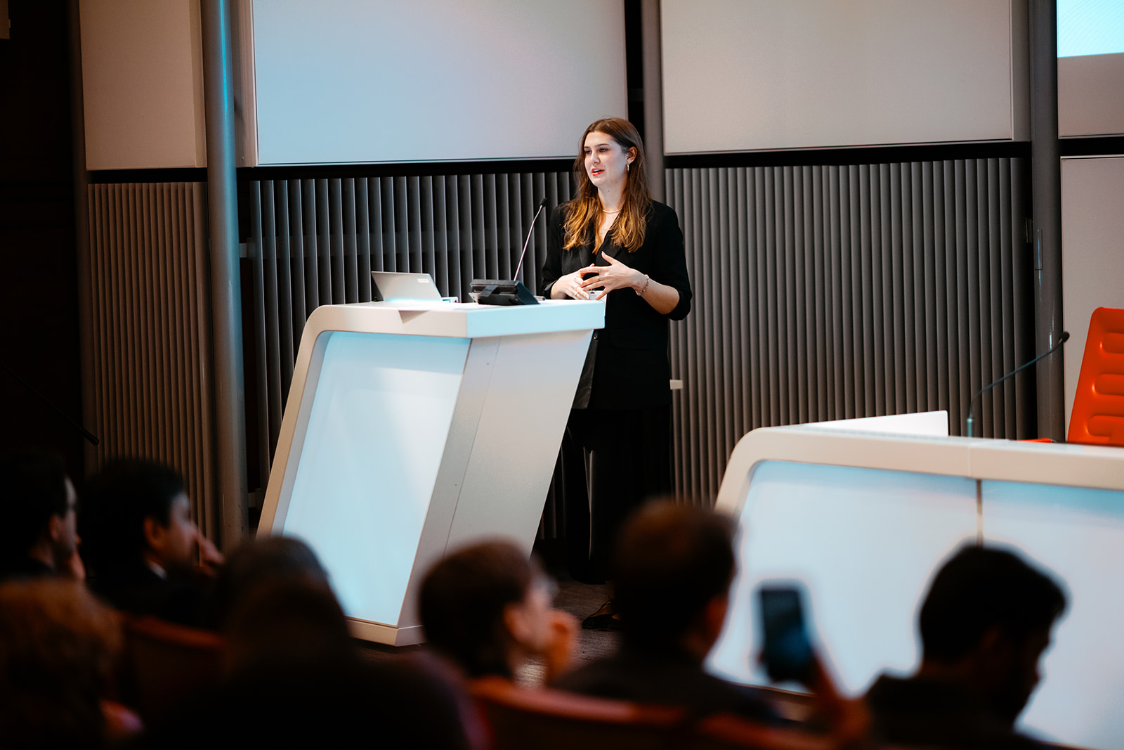
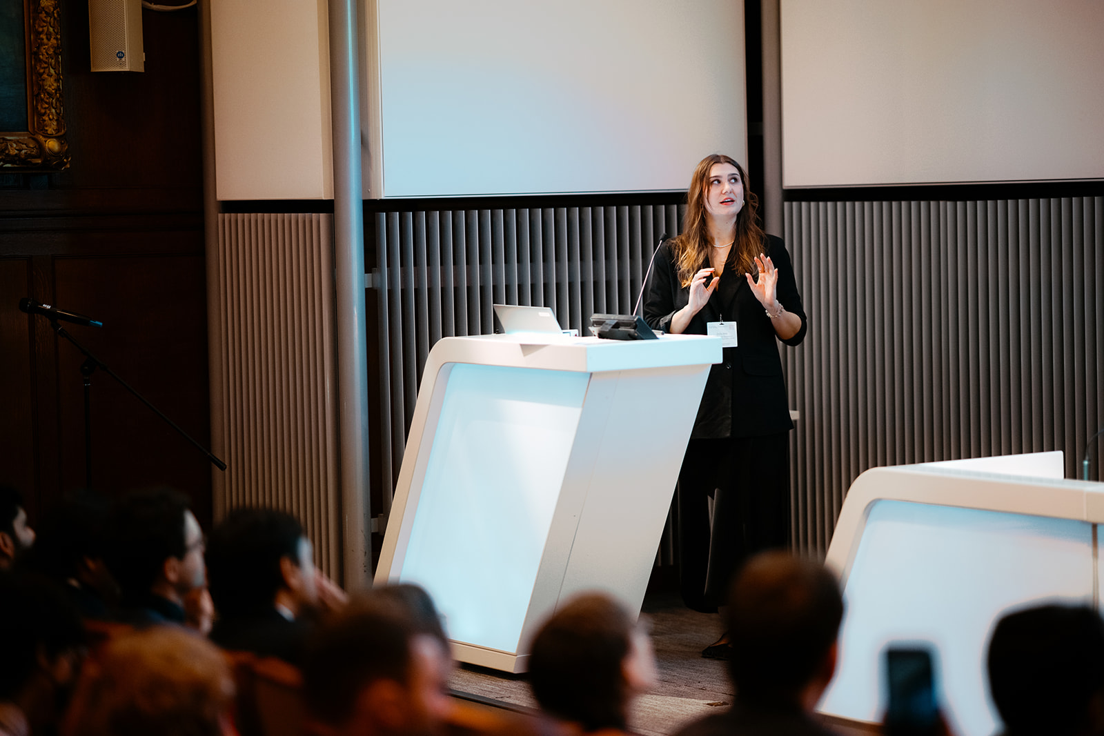
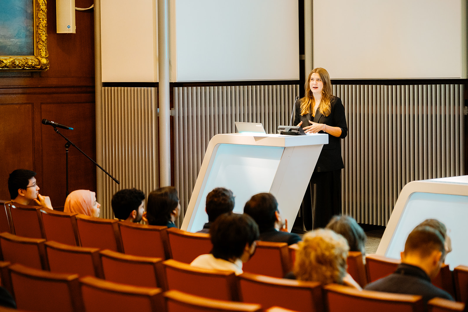
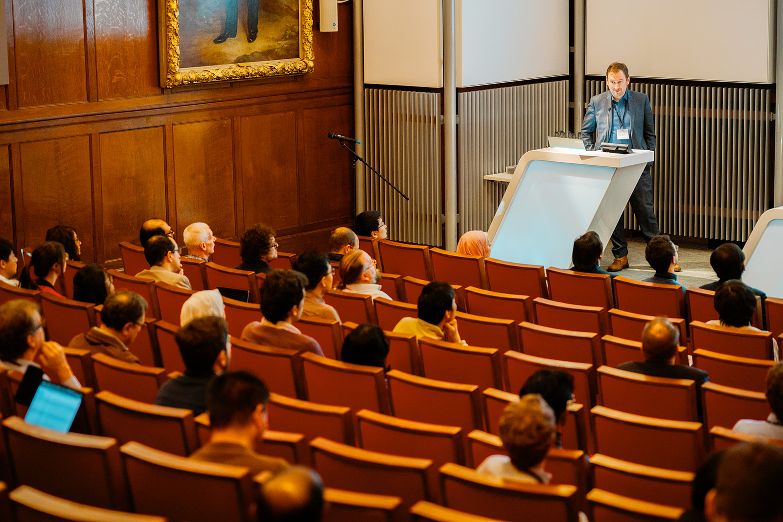
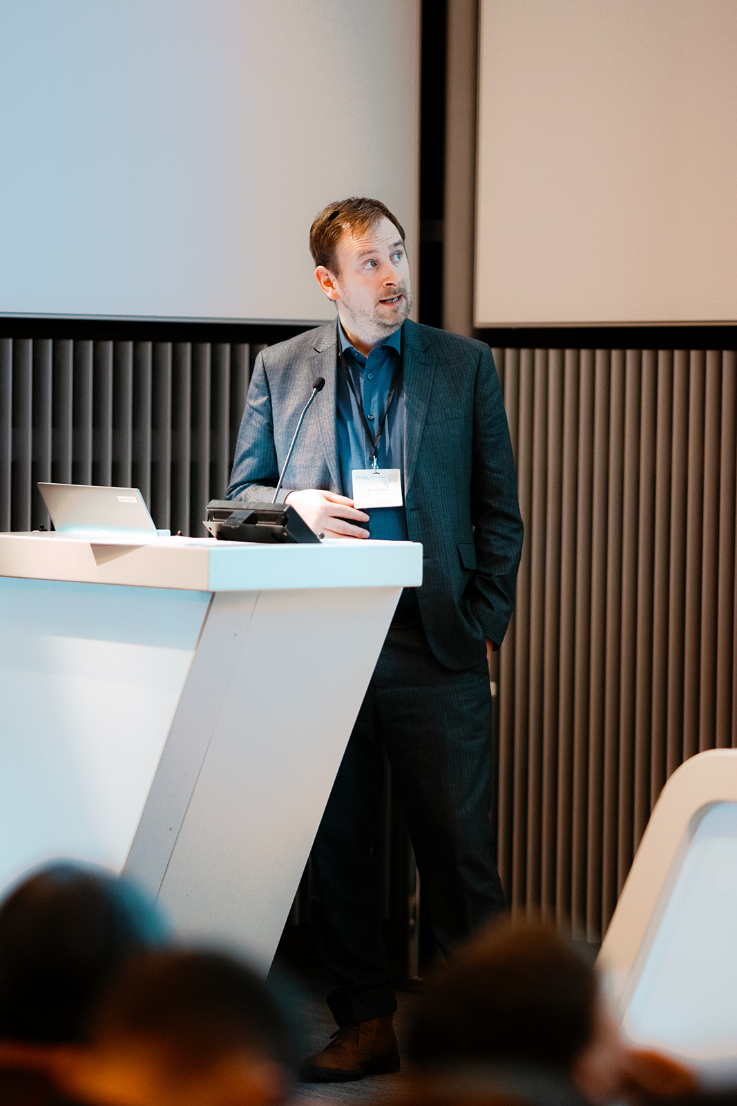
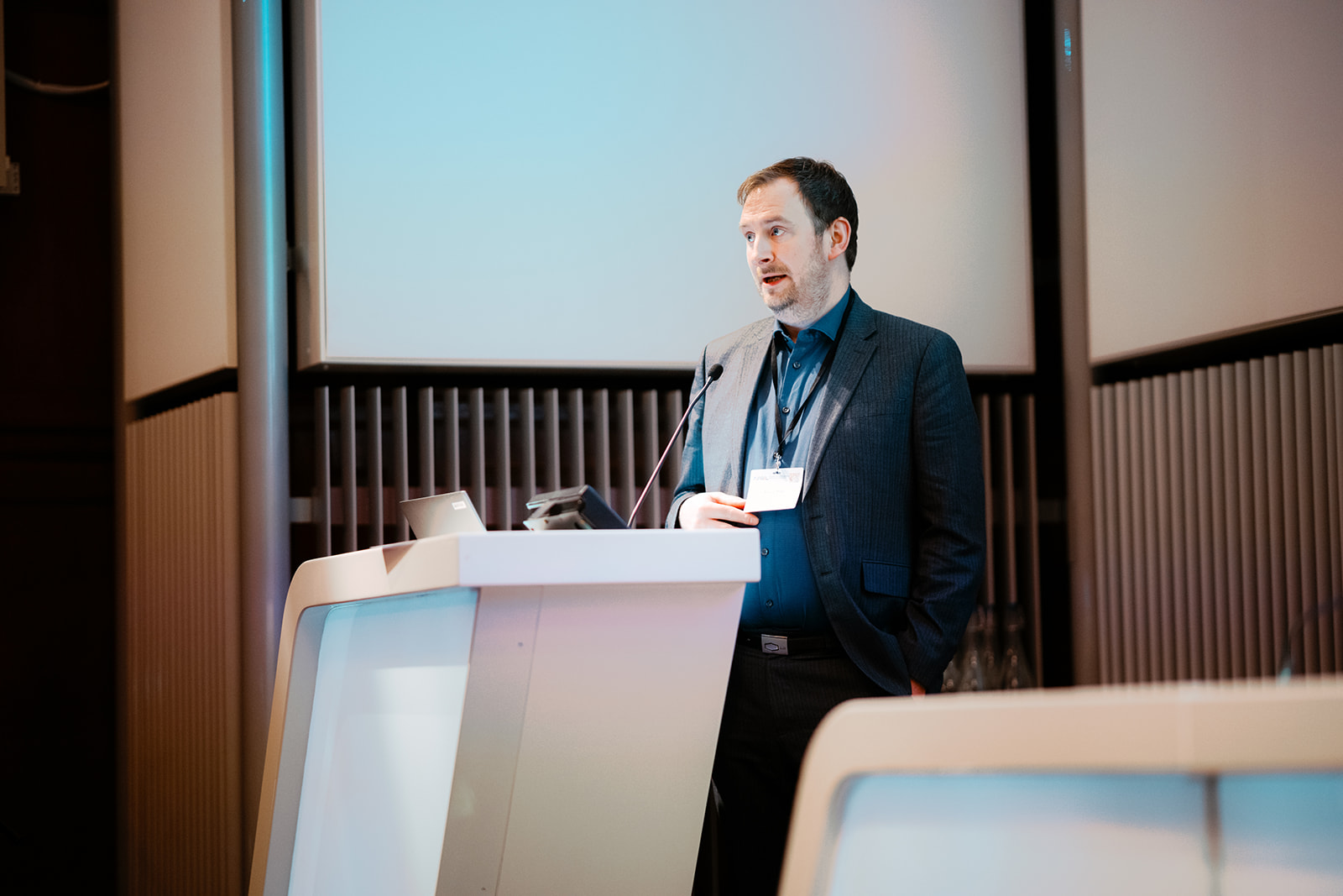
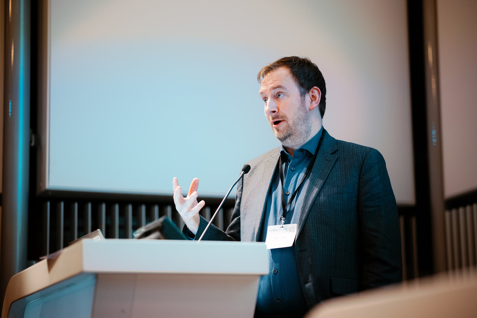
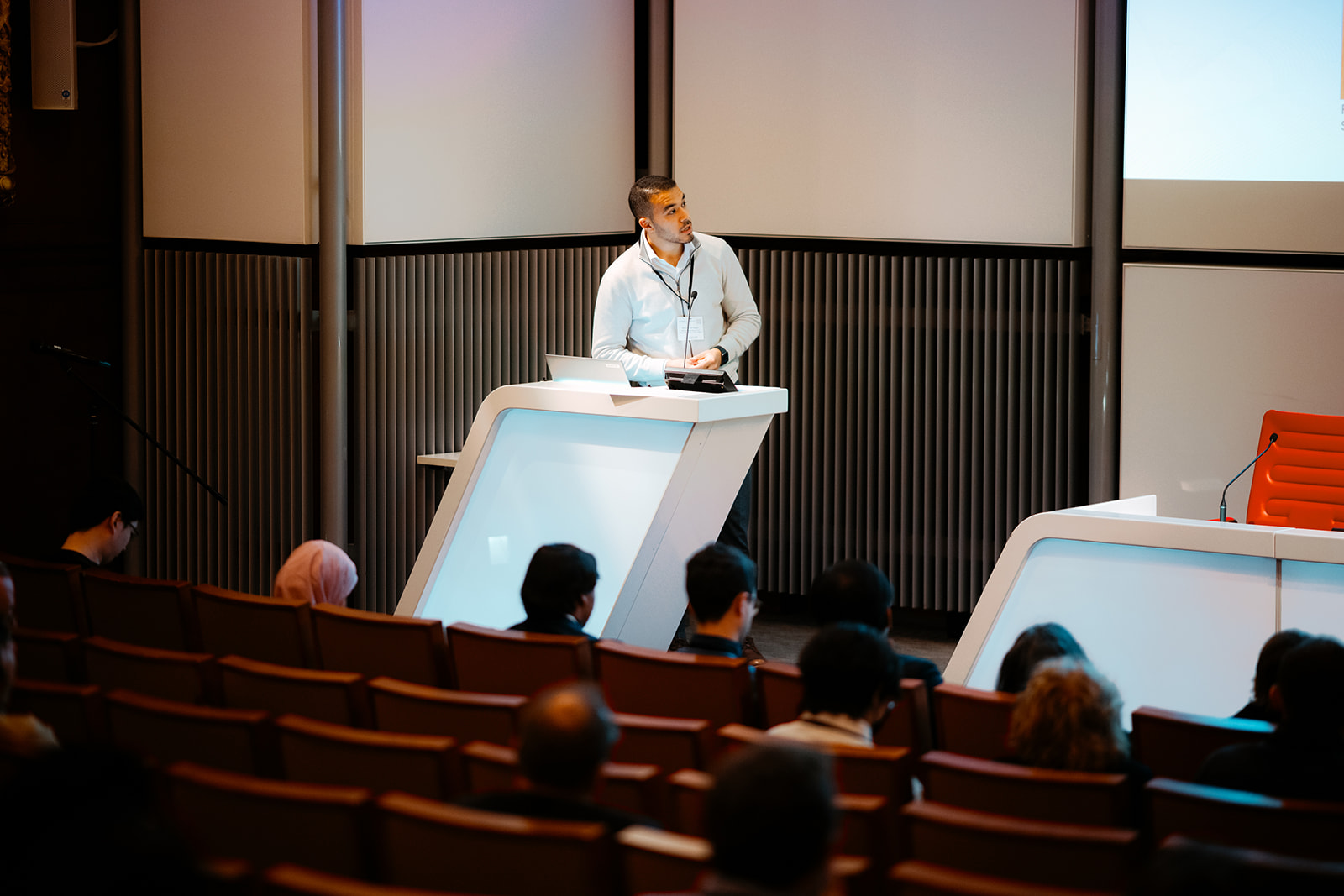
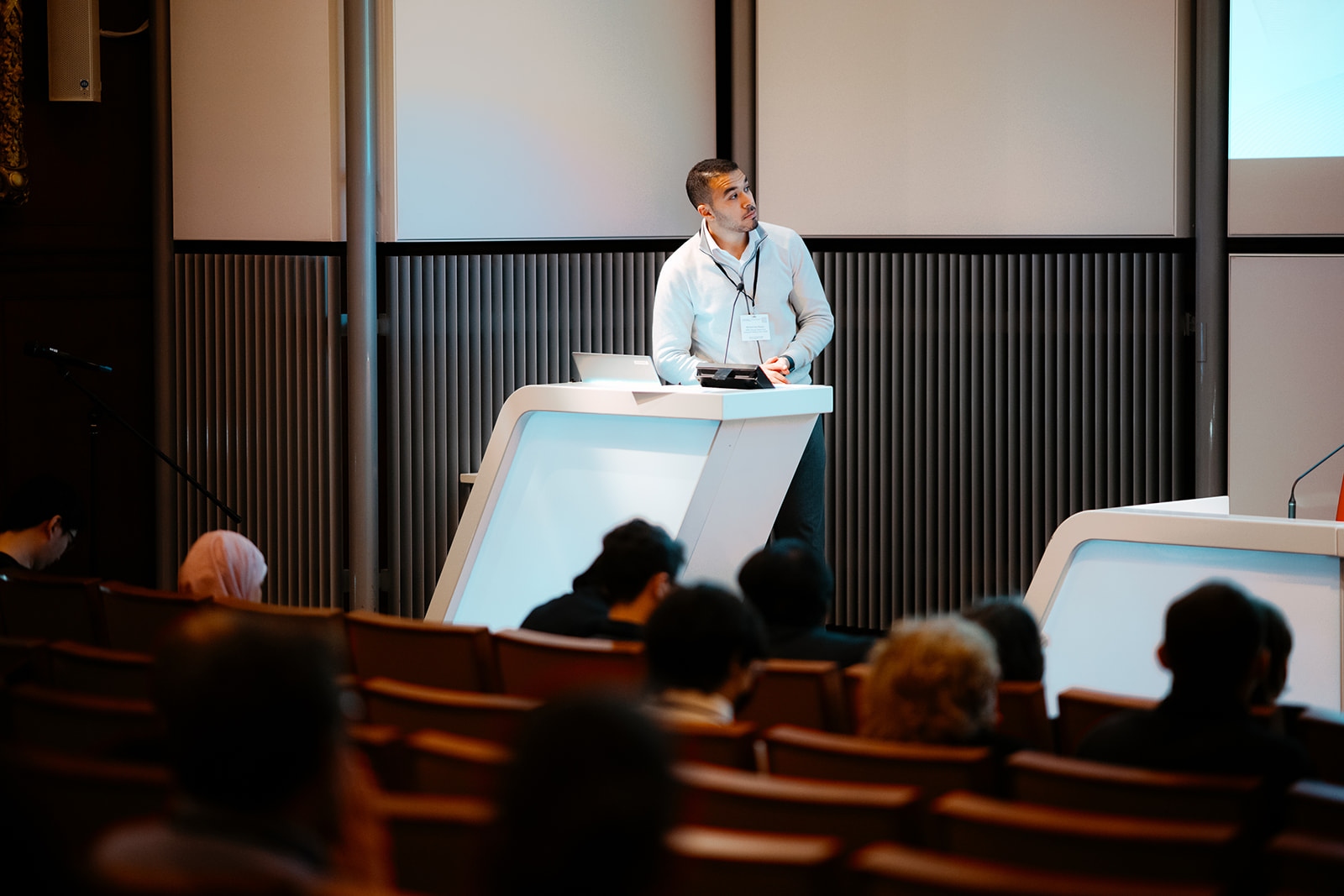
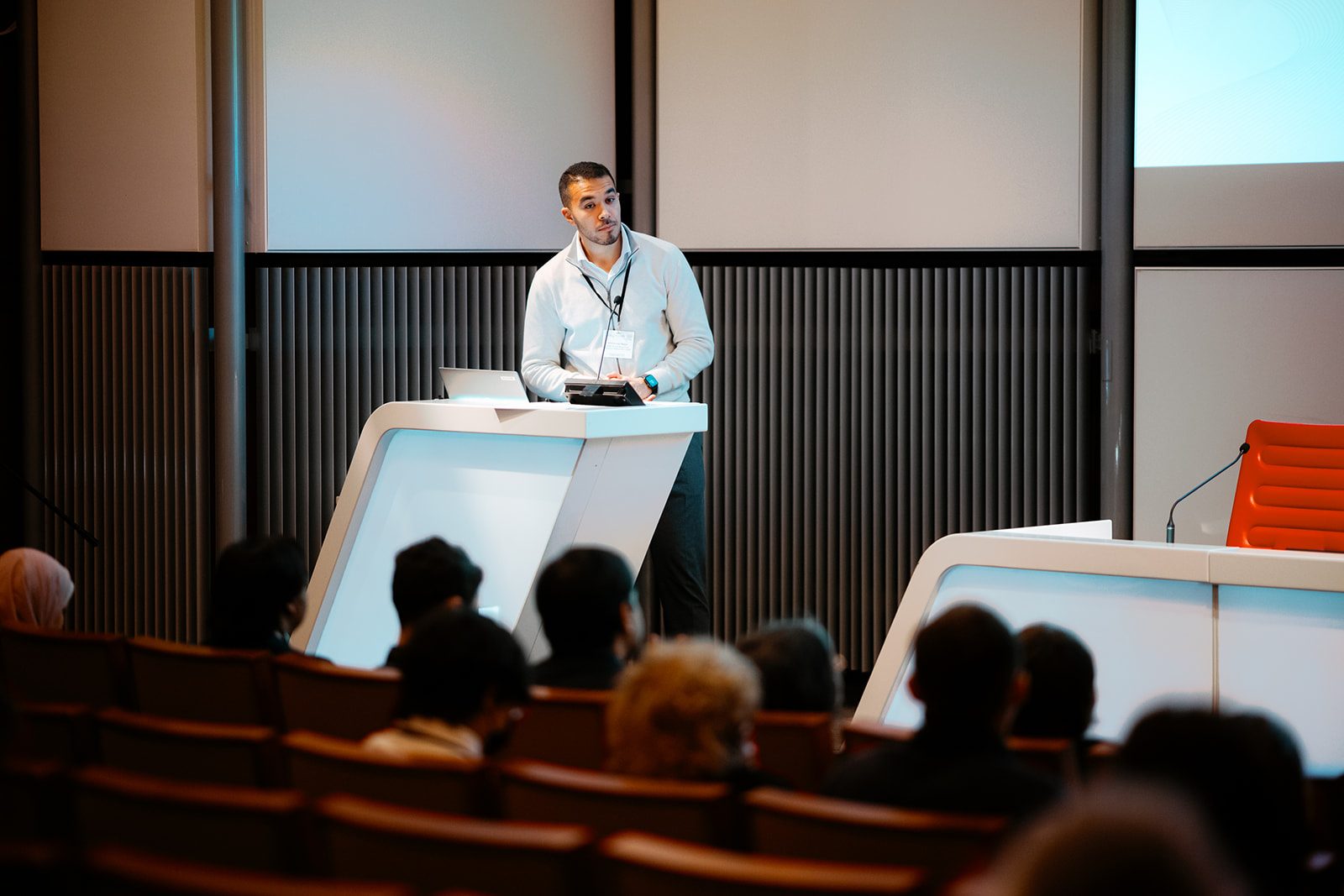
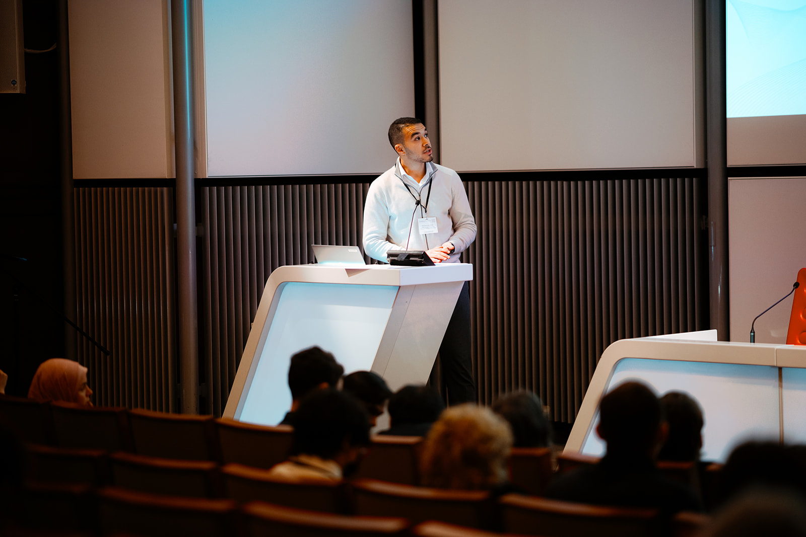
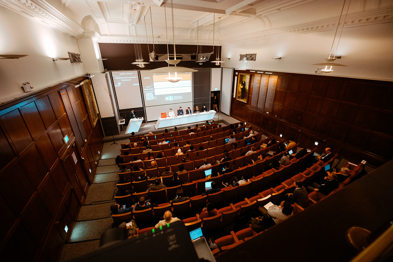
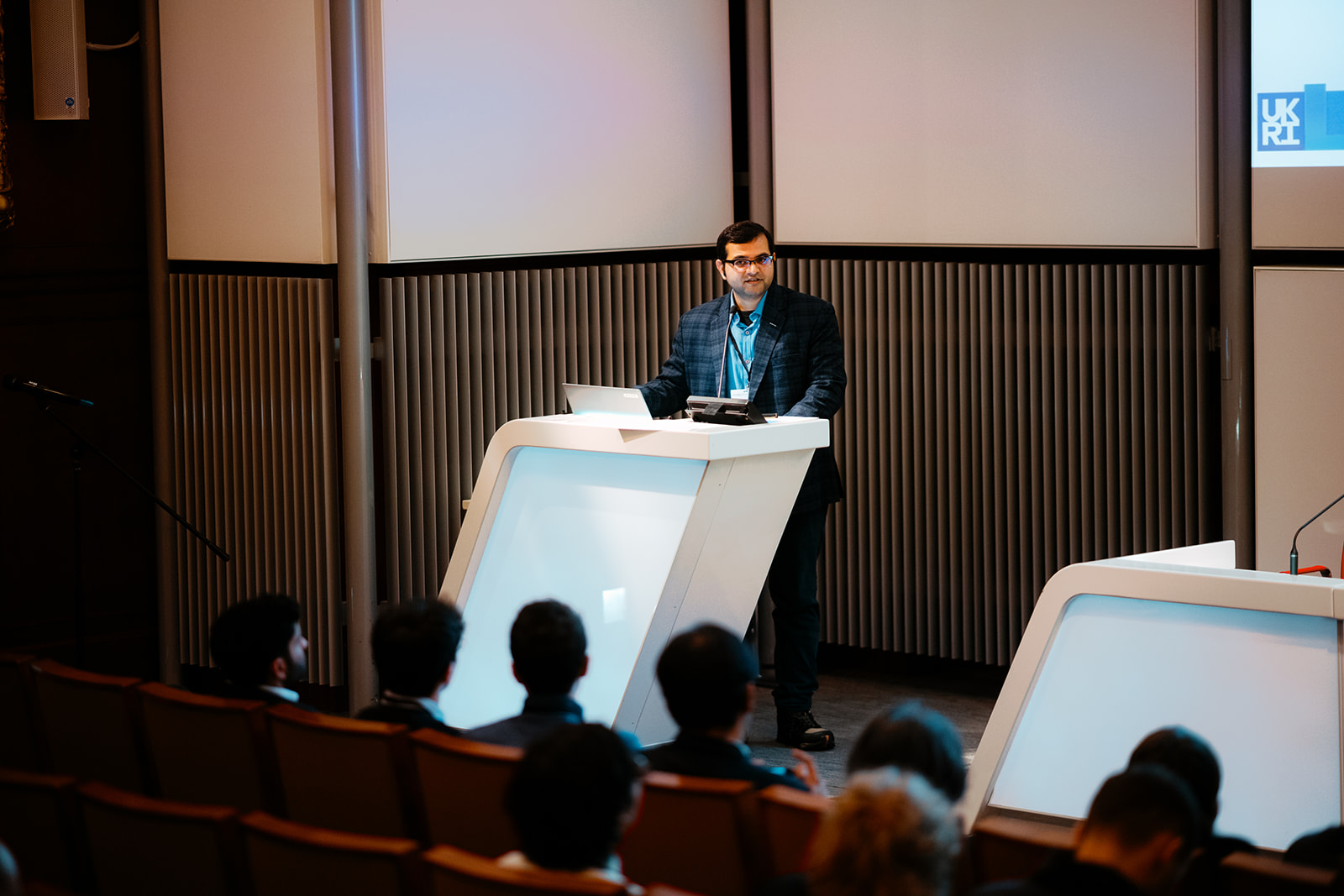
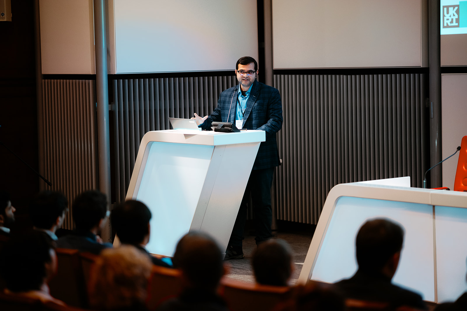
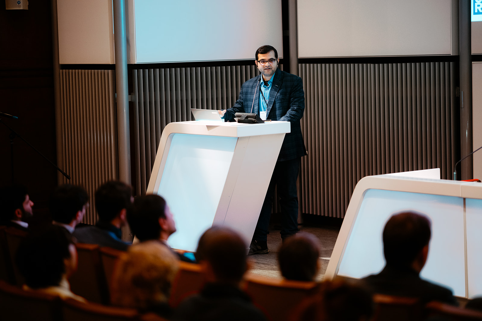
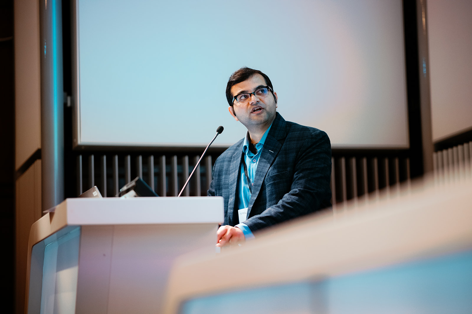
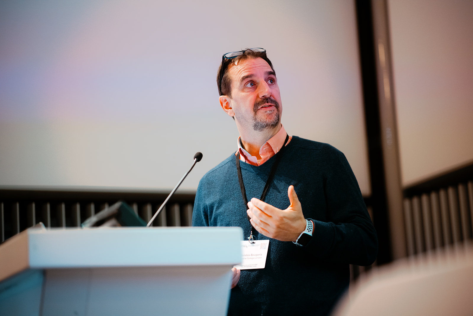
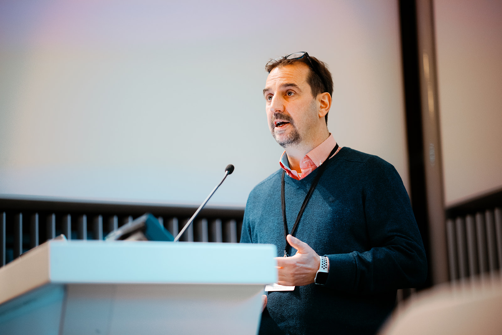
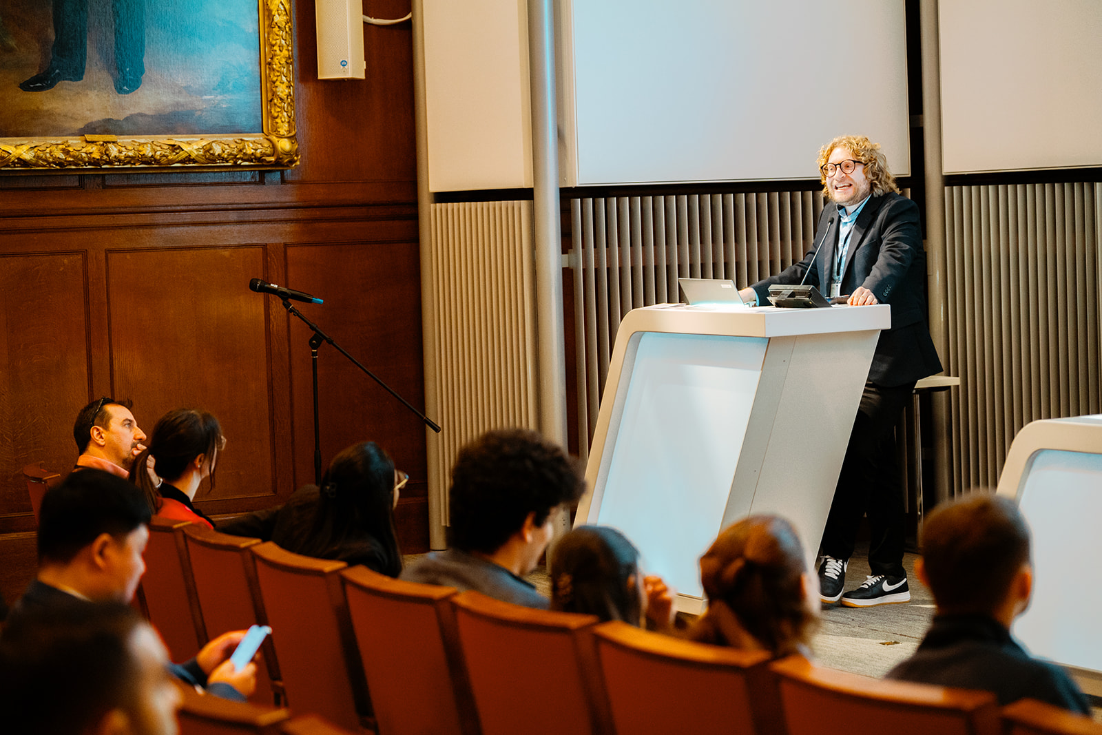
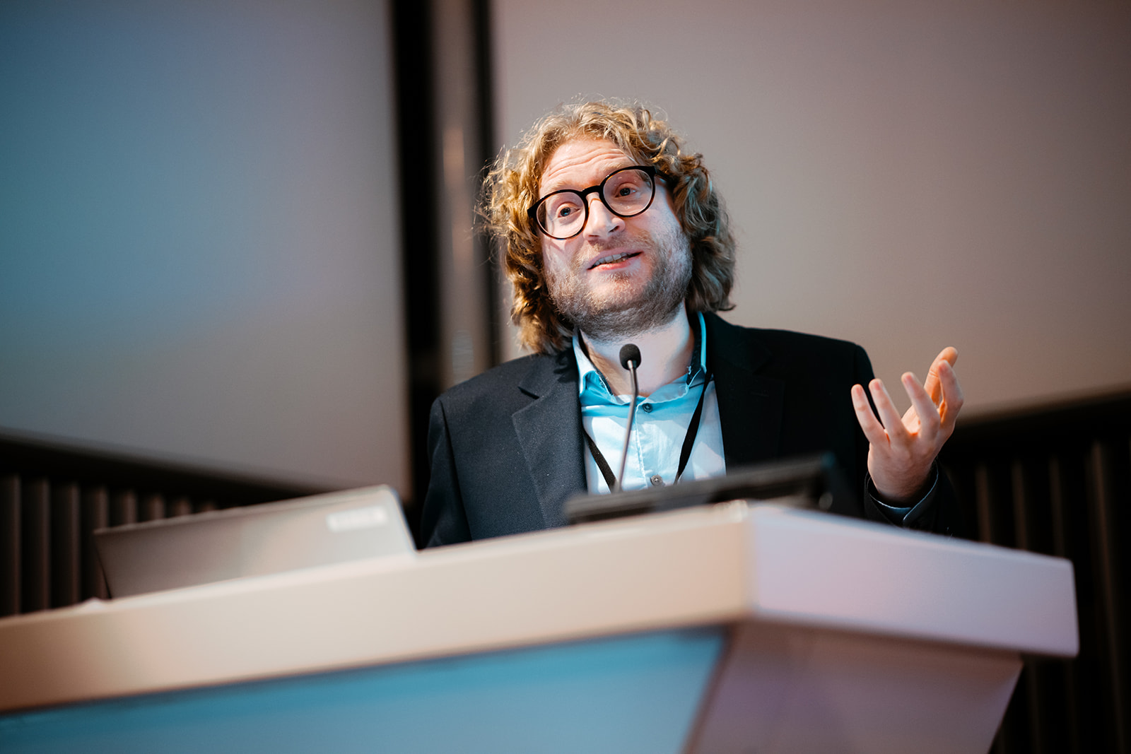
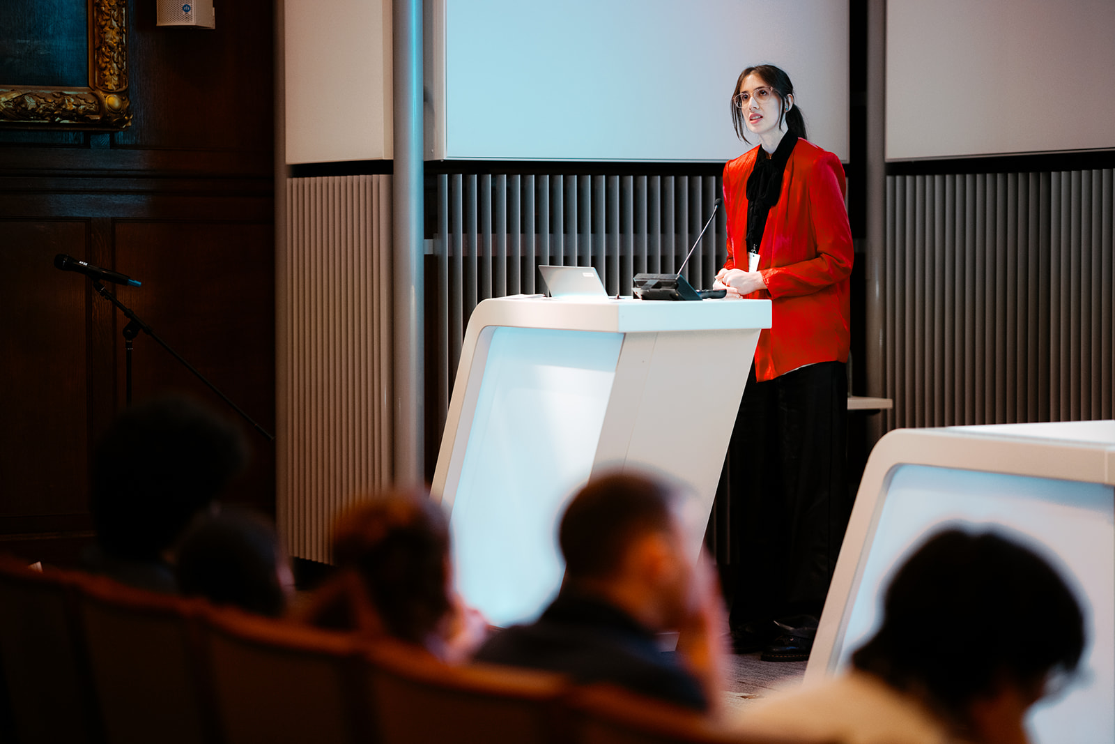
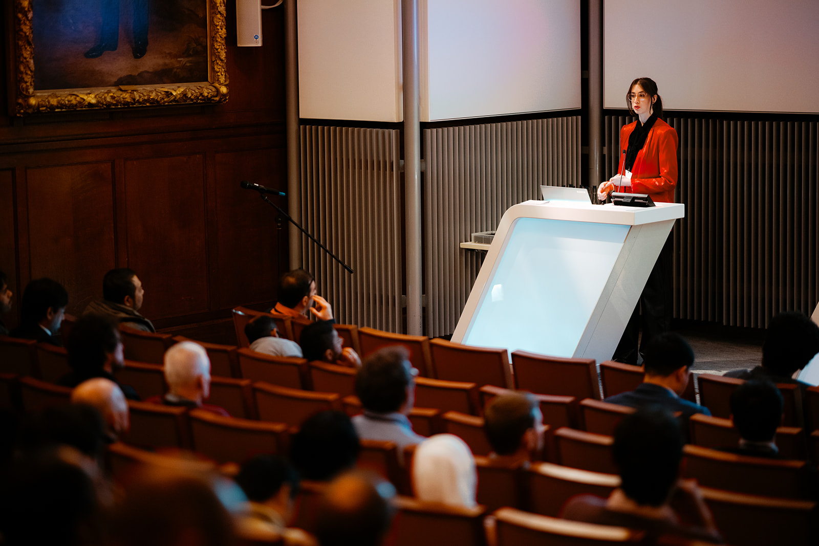
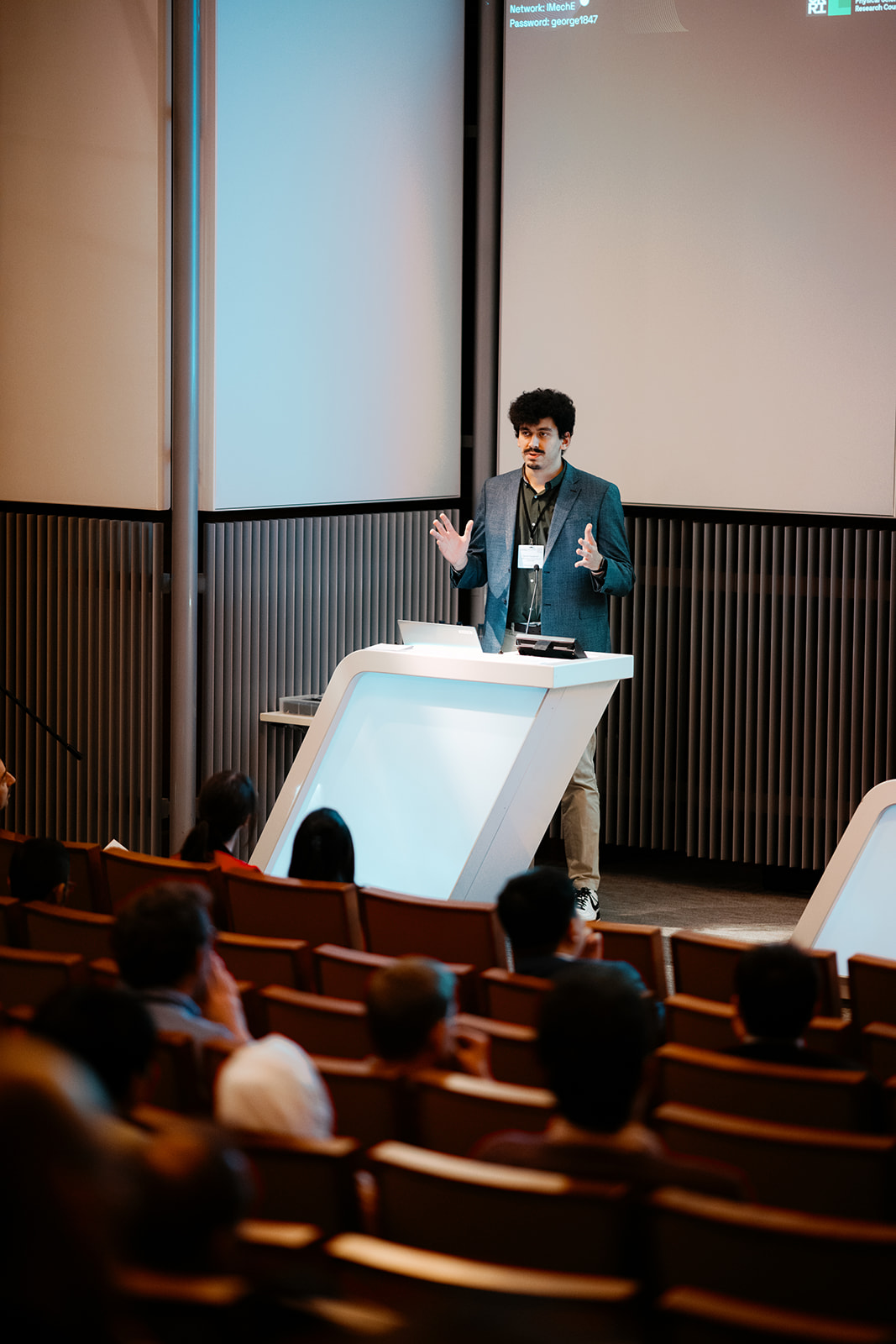
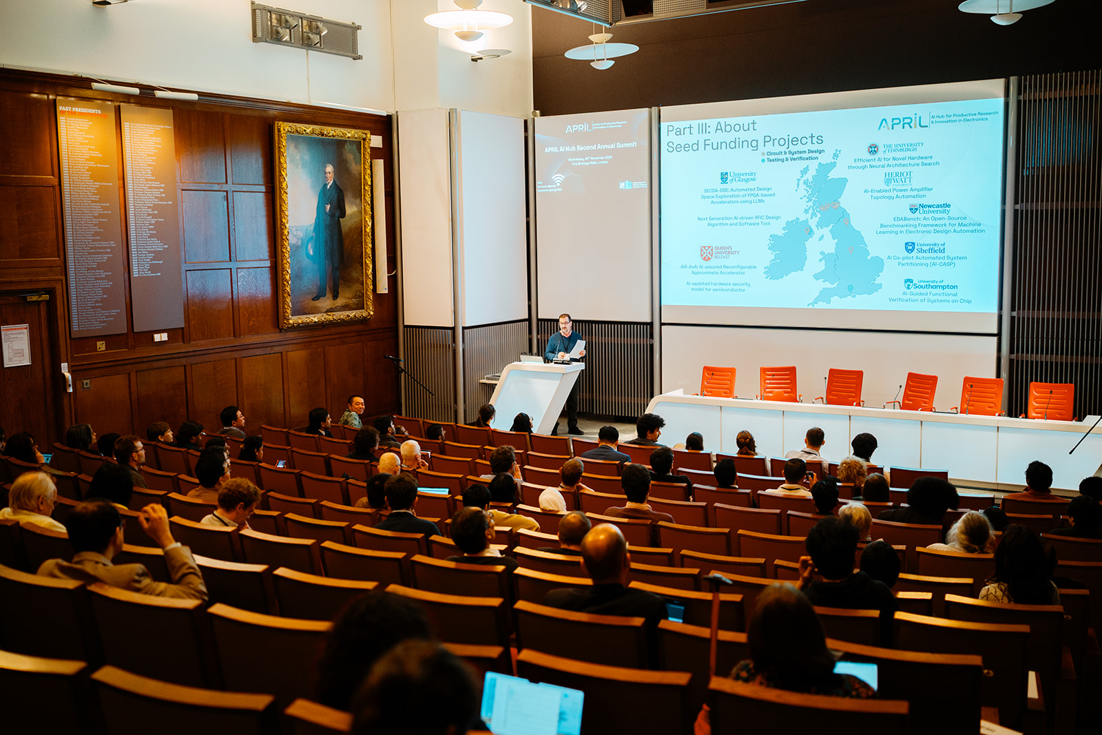
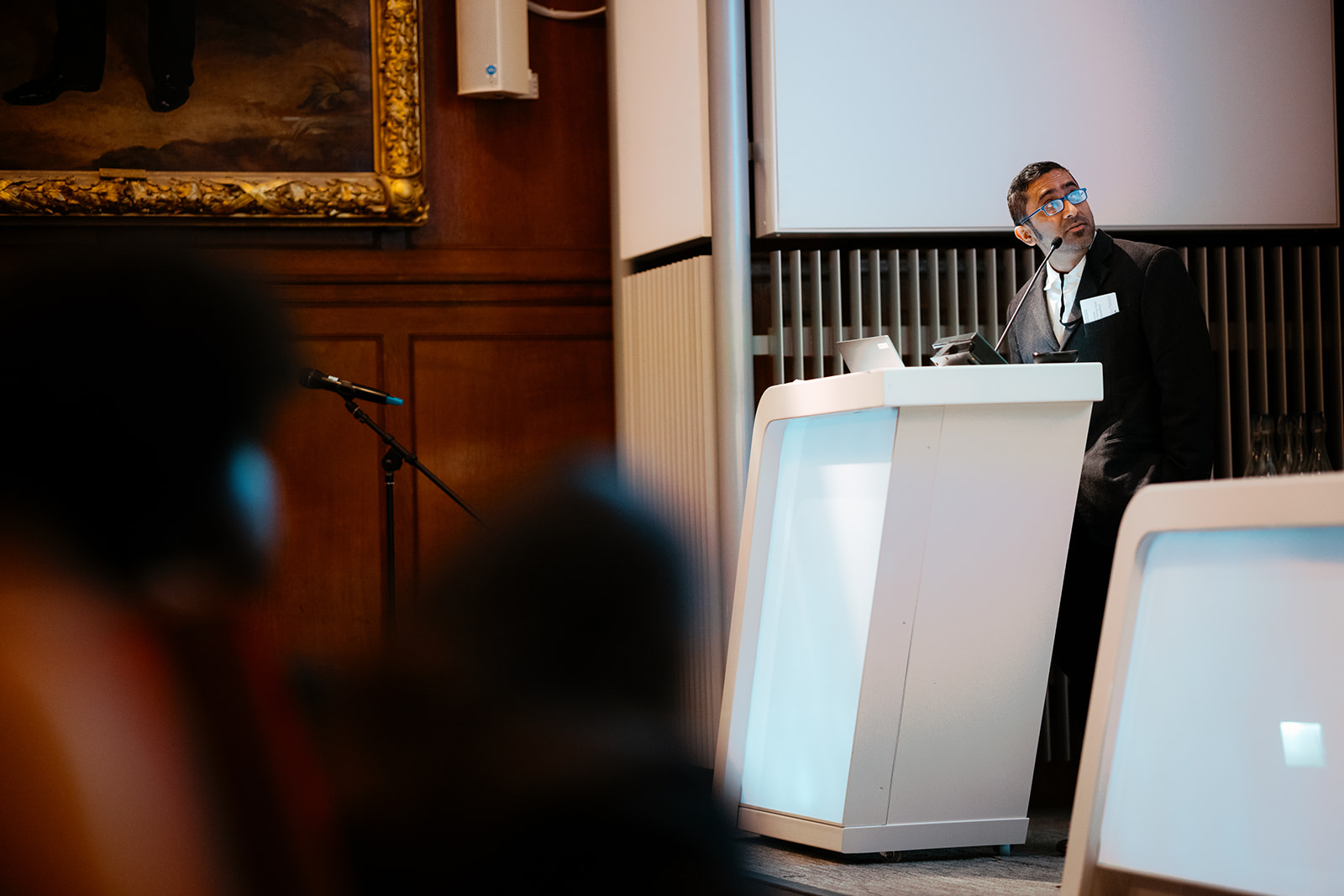
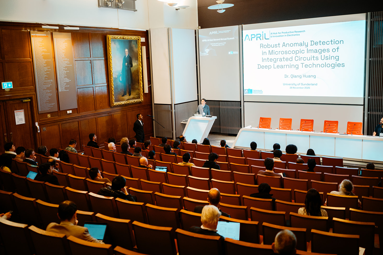
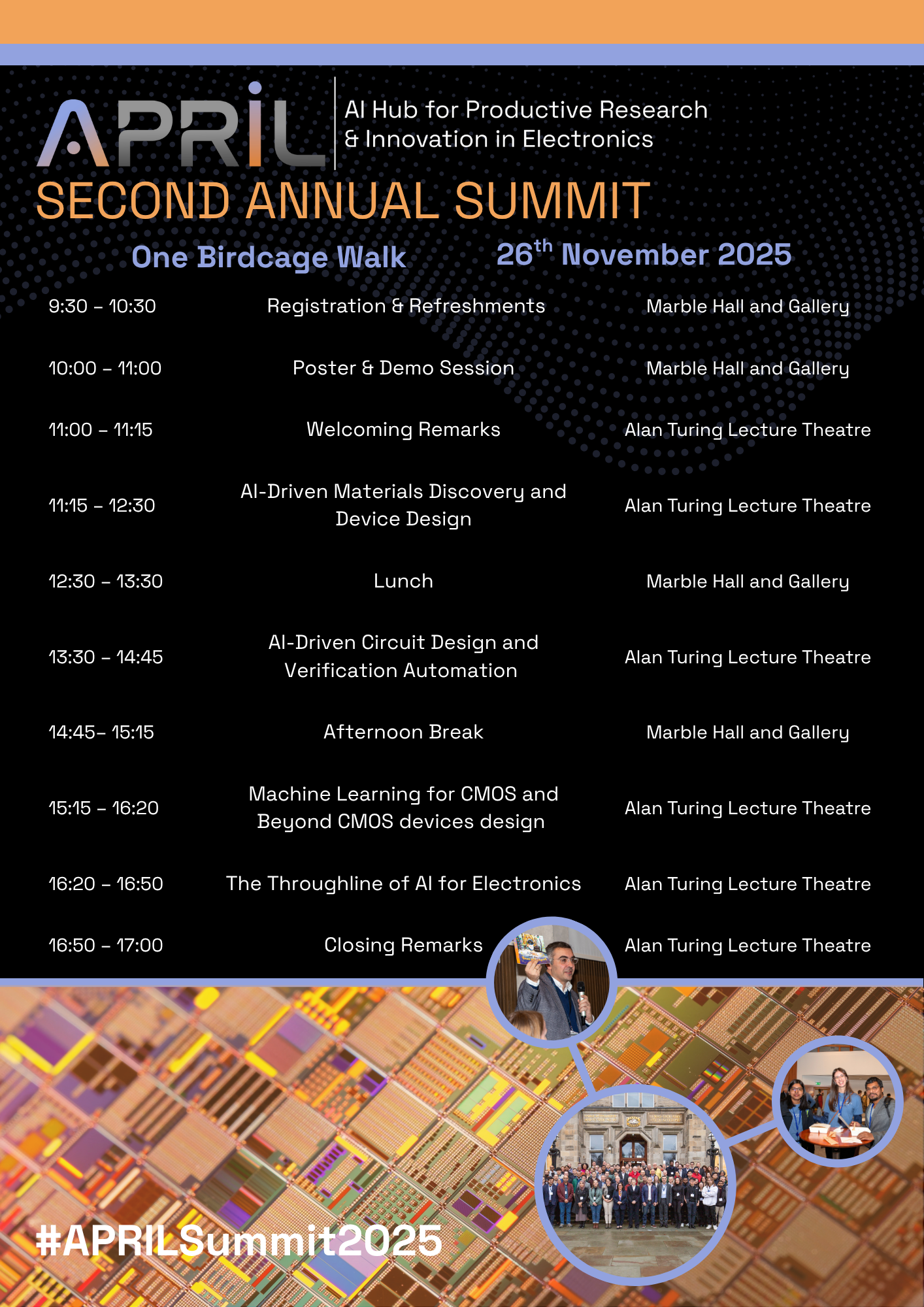
APRIL AI Hub Second Annual Summit
09:30 - 17:00 One Birdcage Walk, London
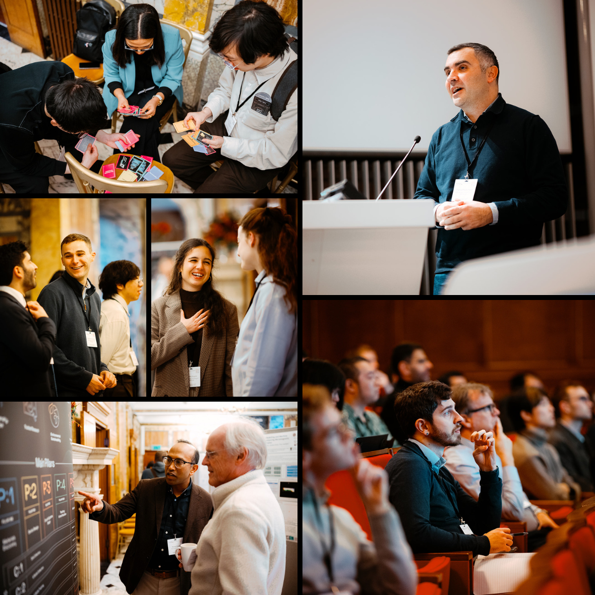
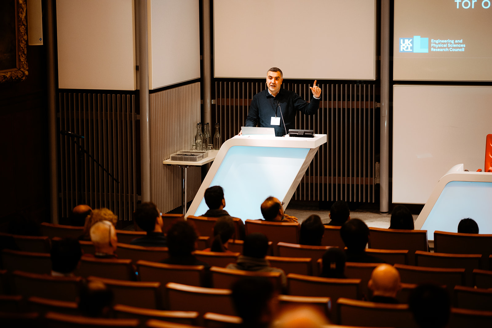
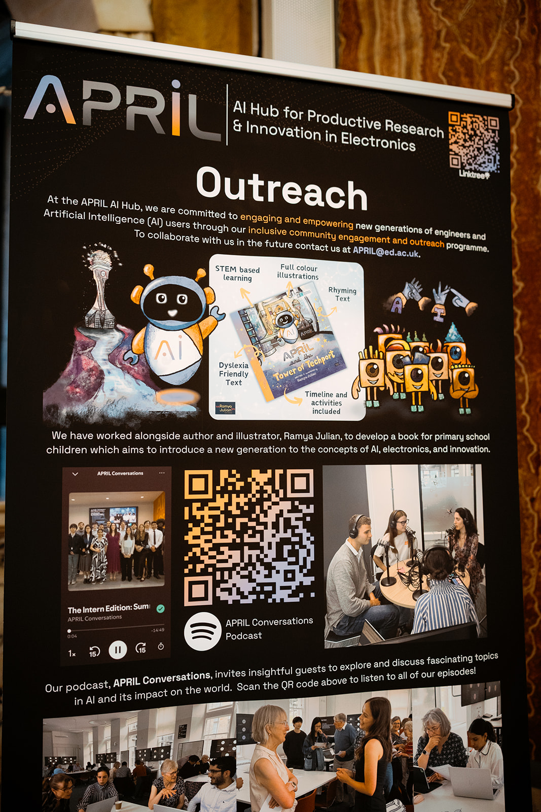
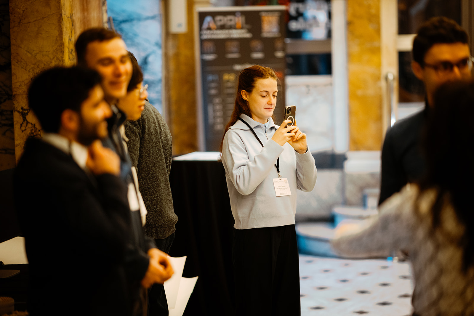
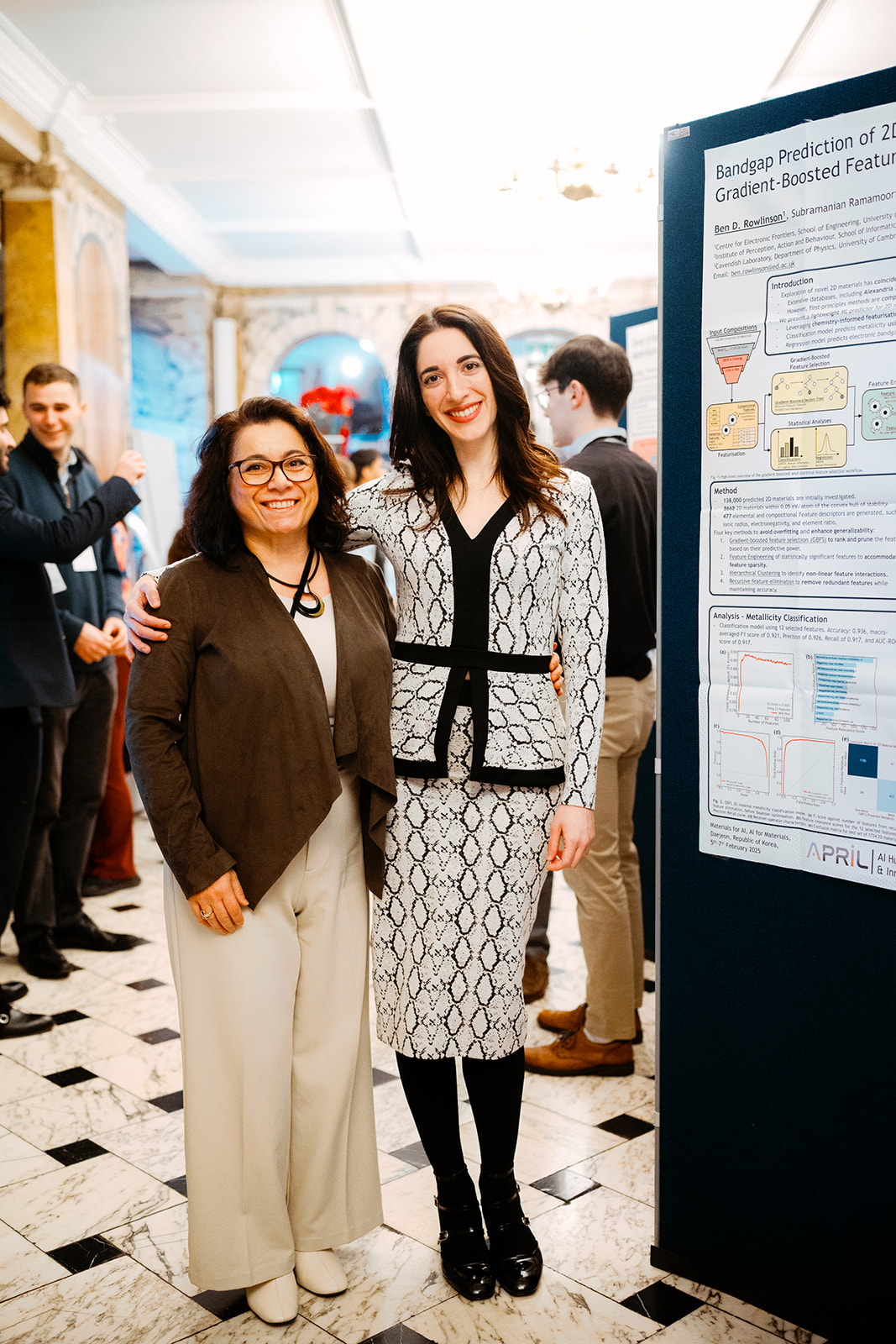
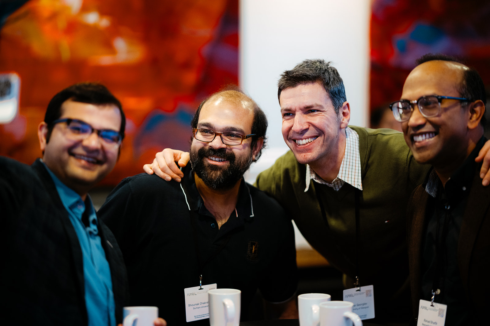
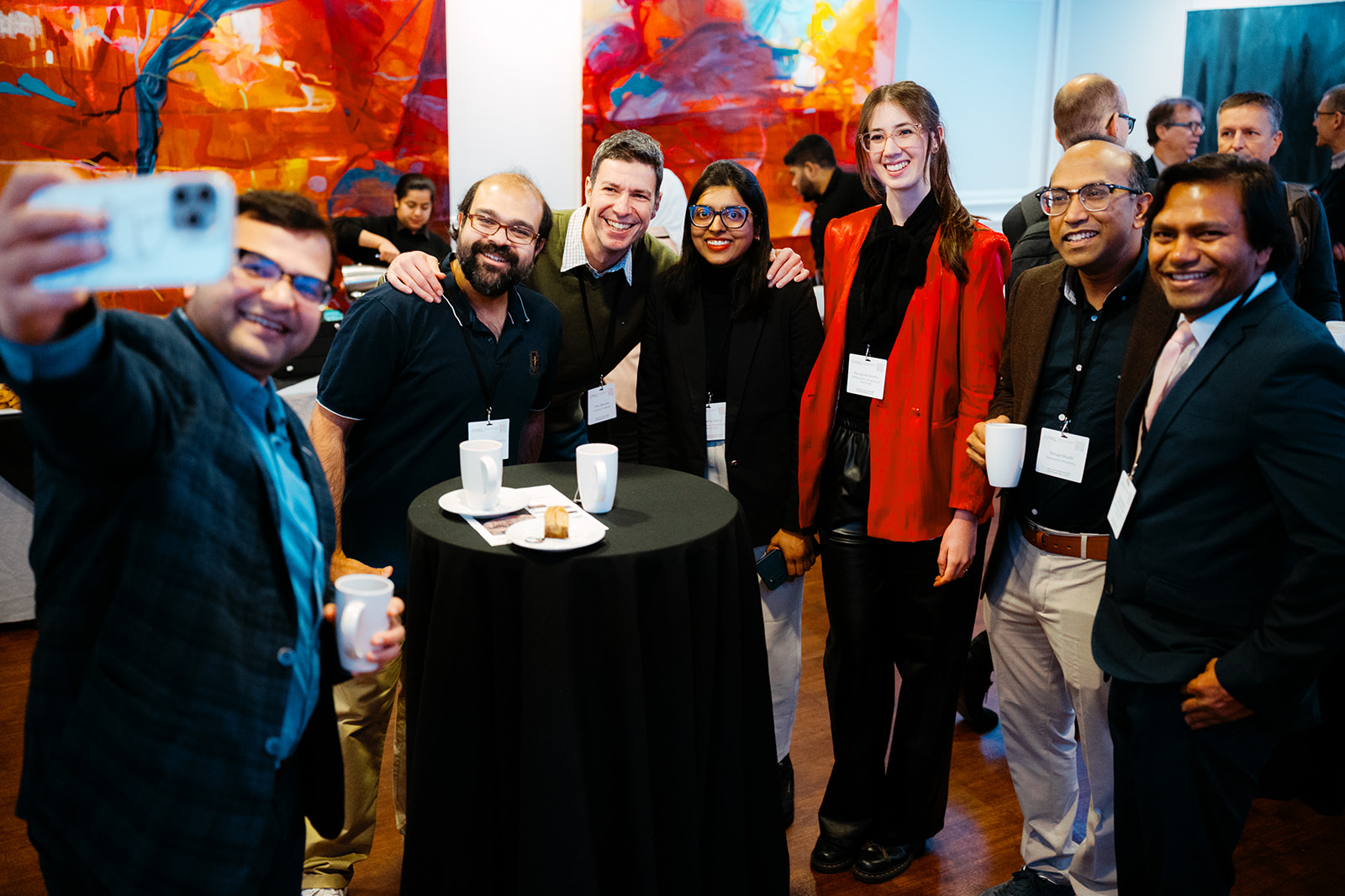
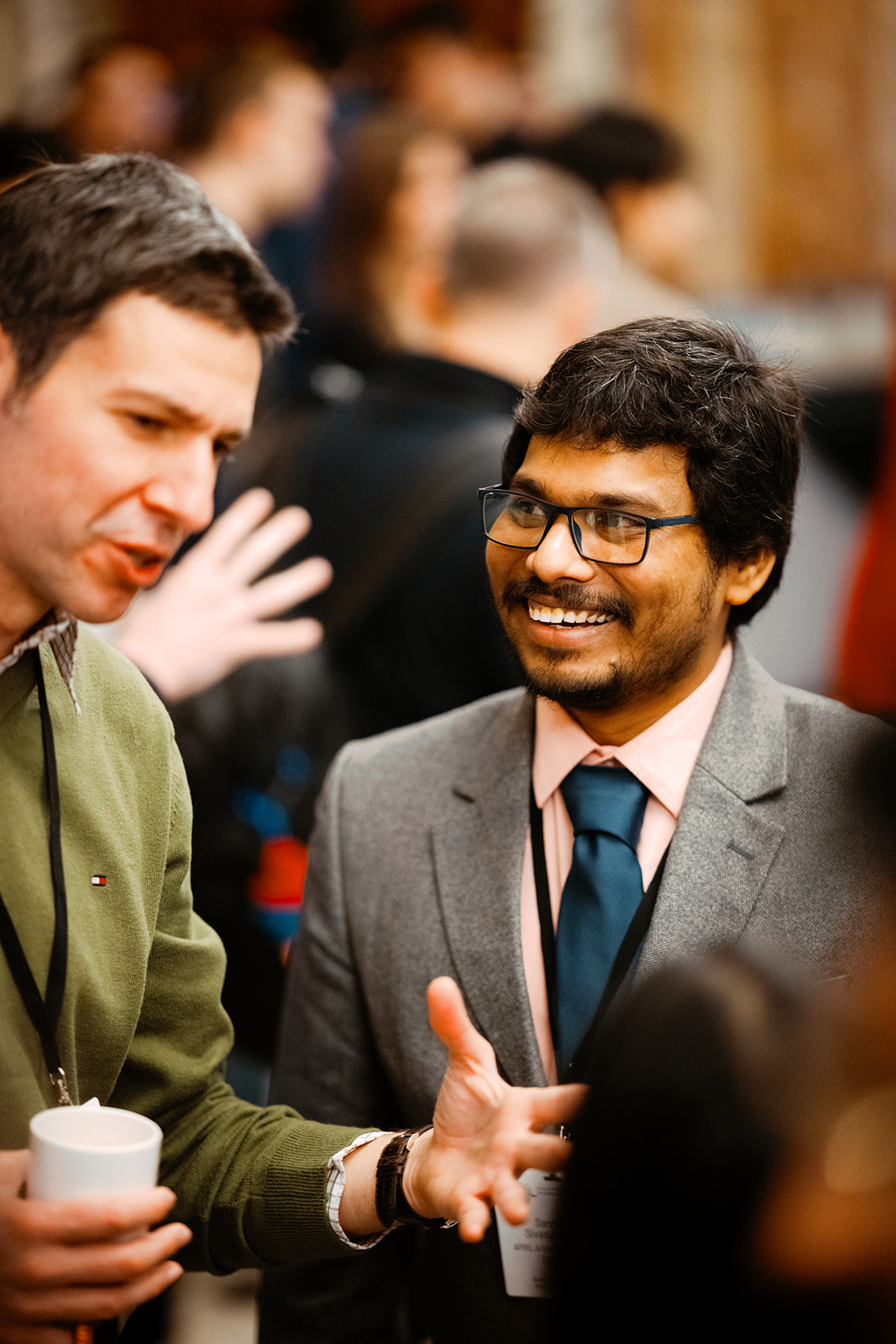
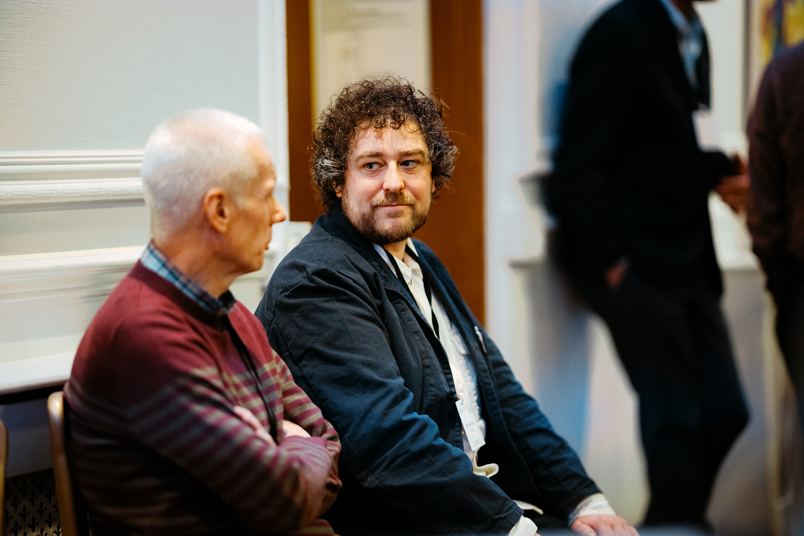
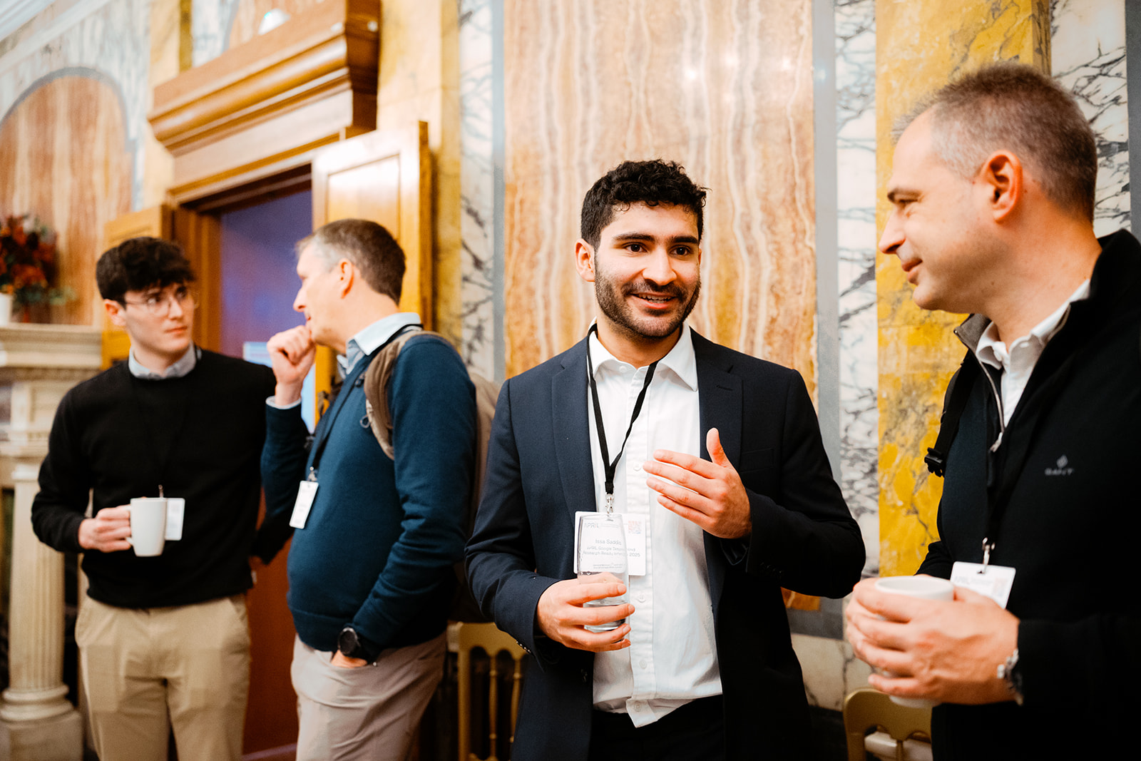
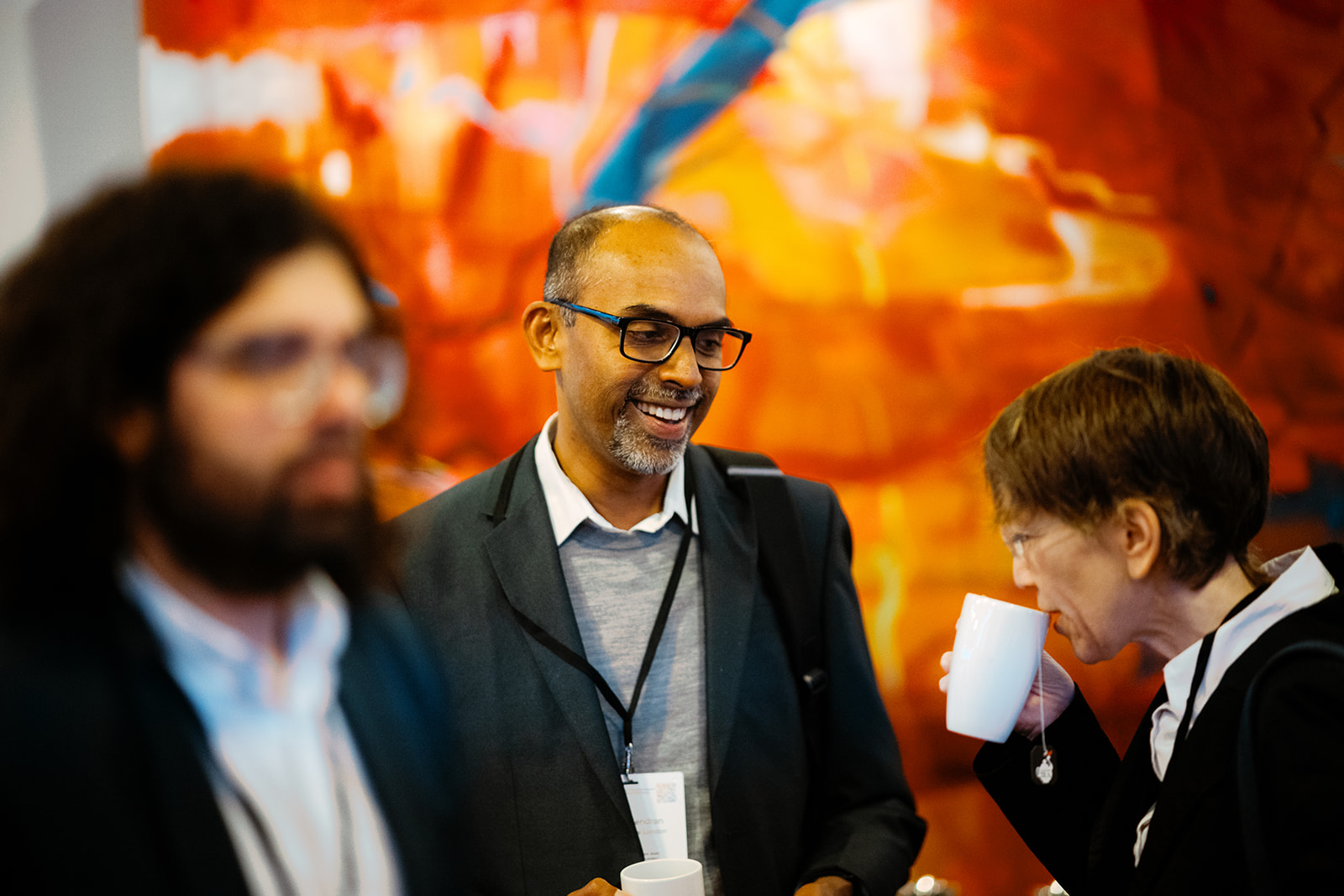
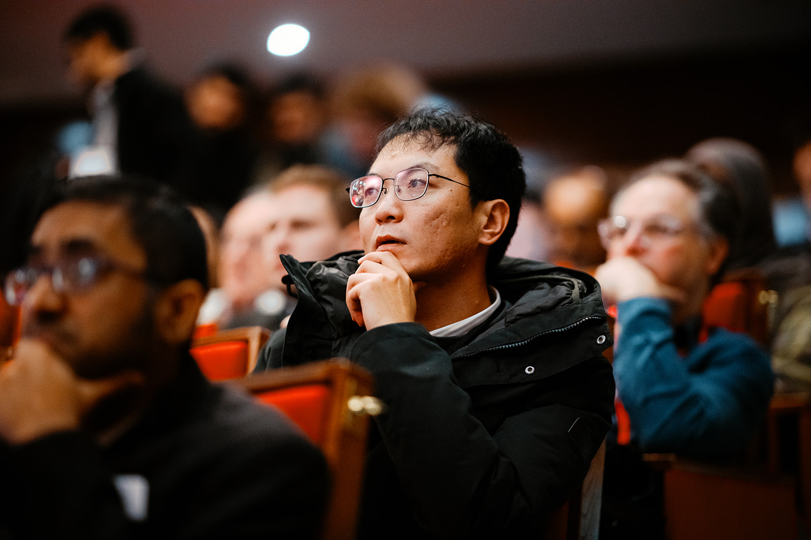
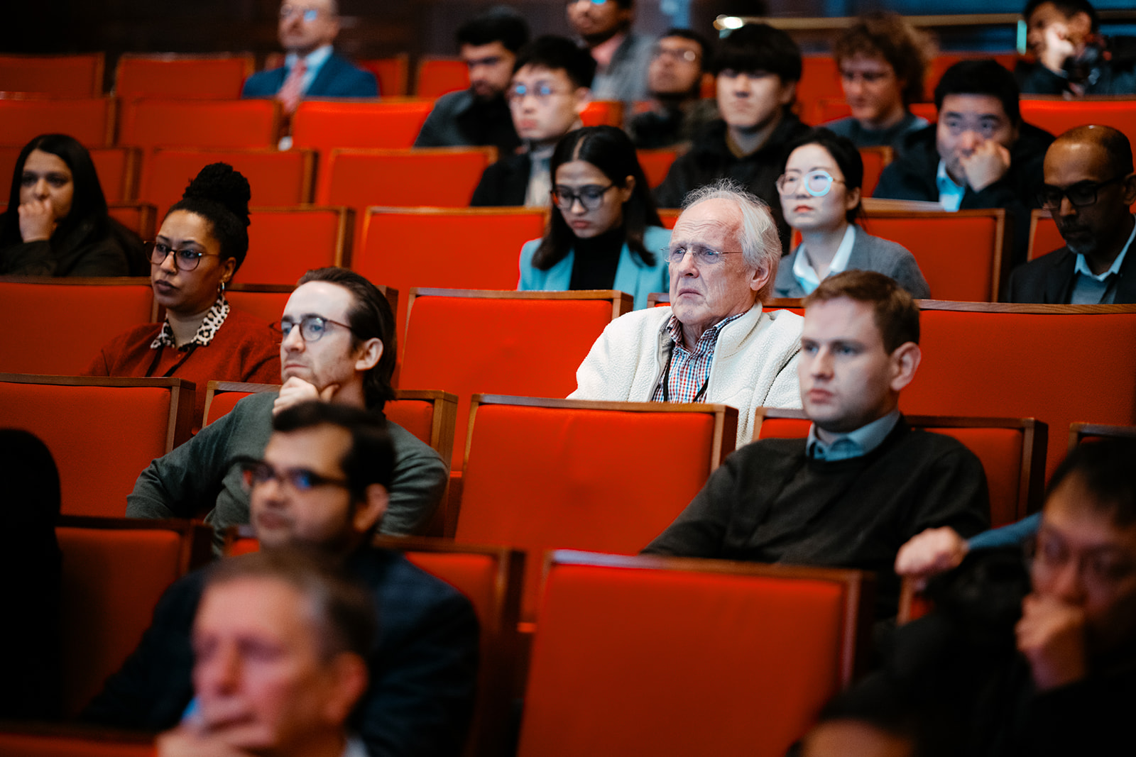
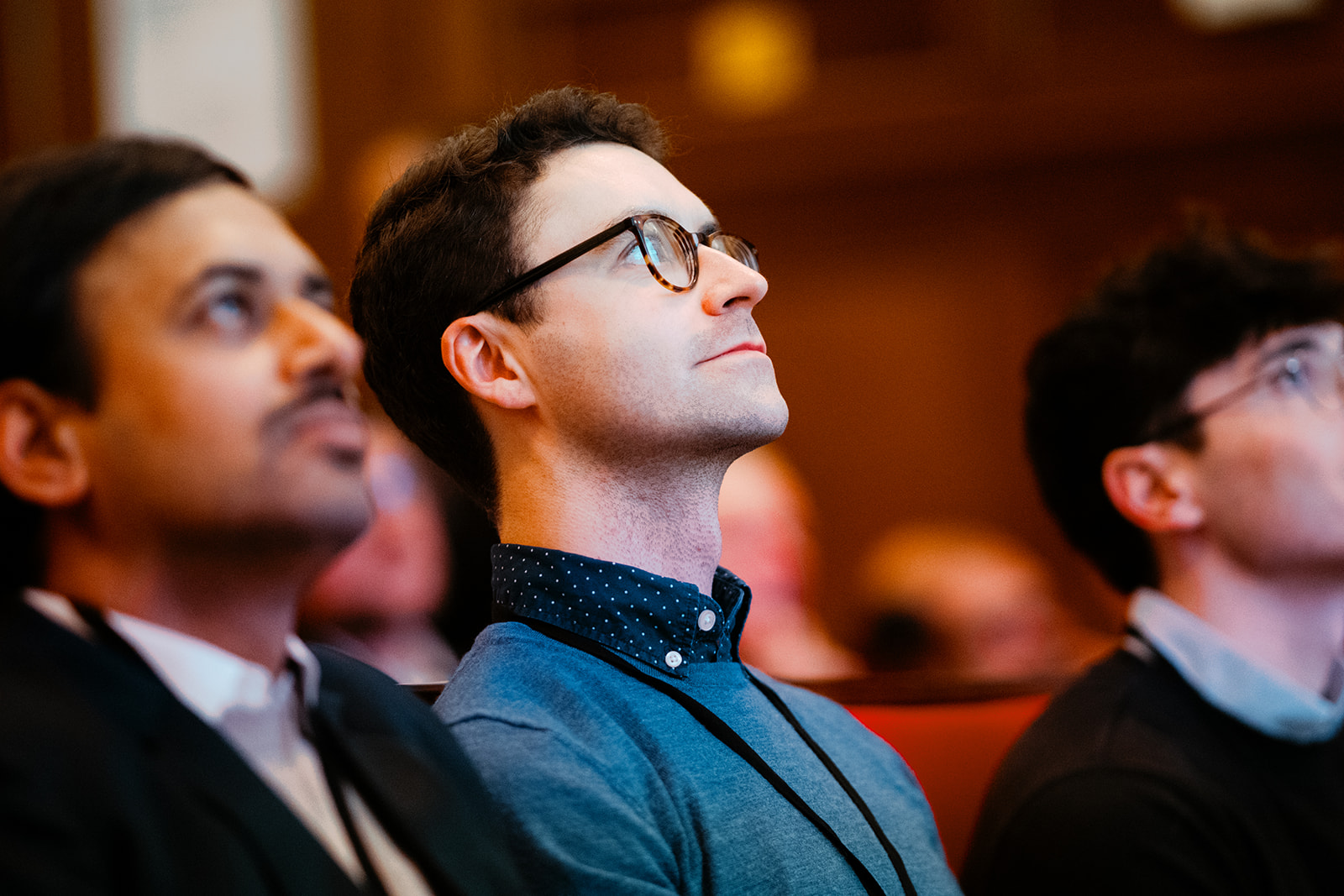
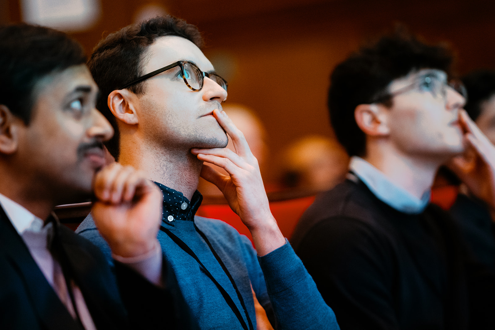
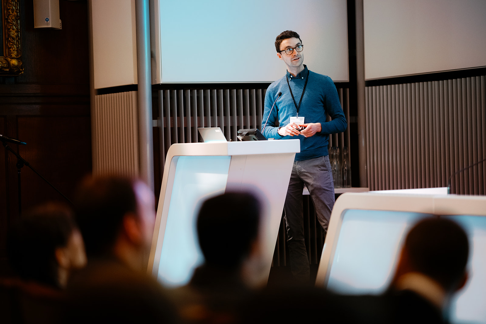
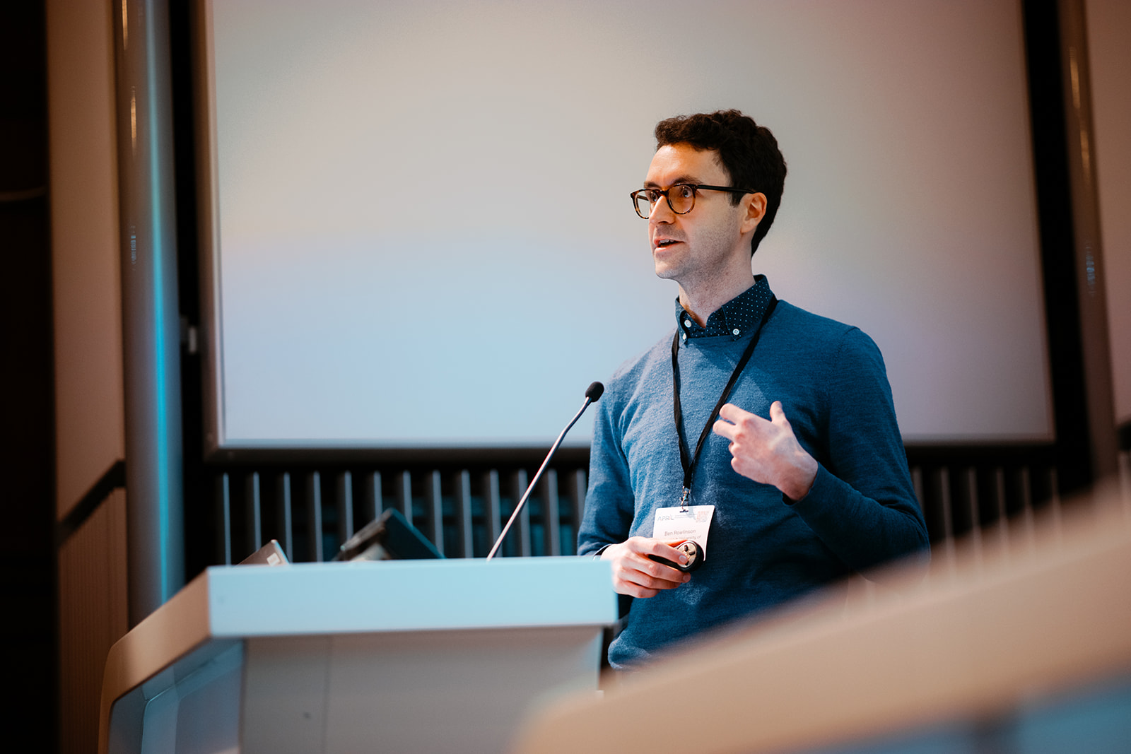
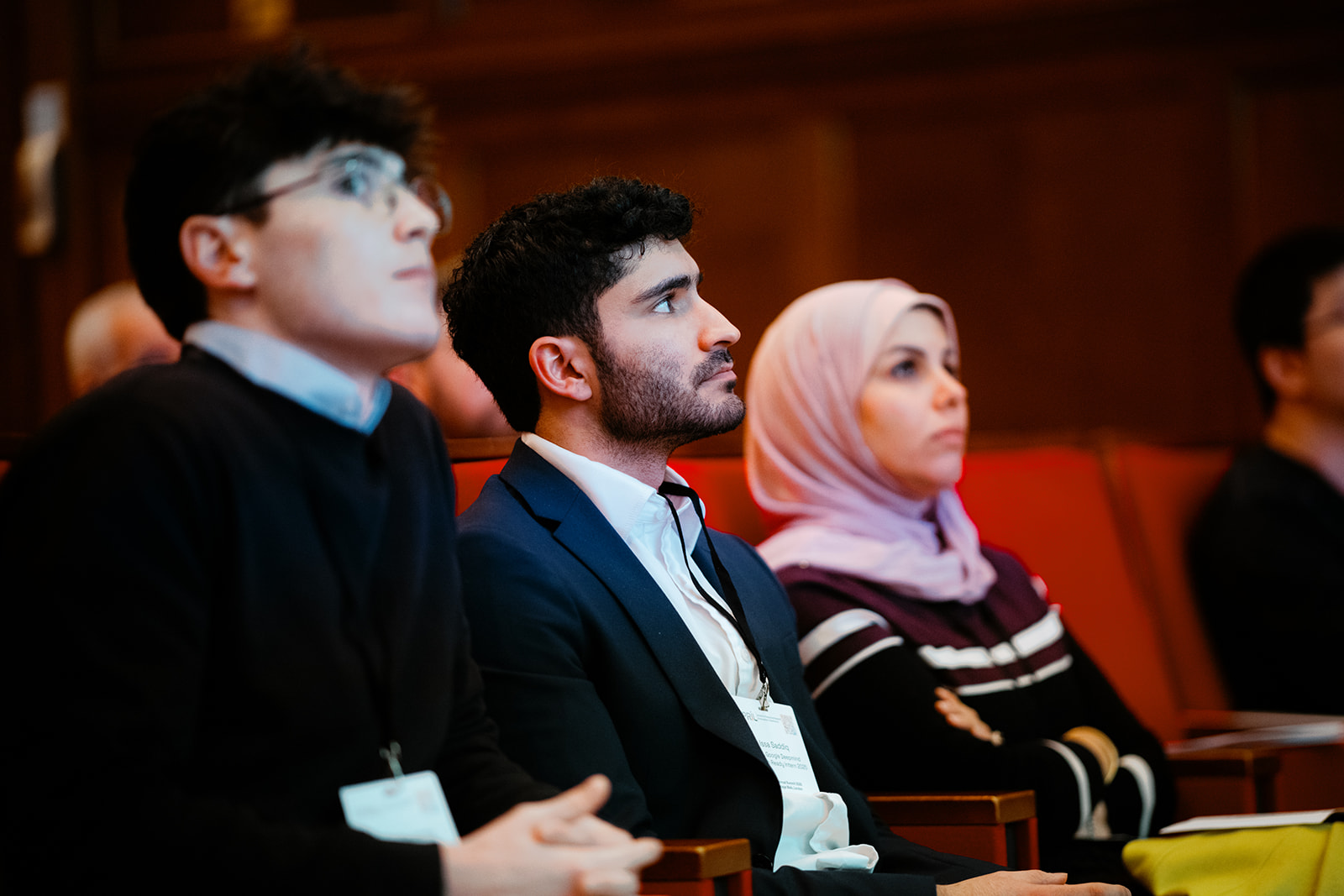
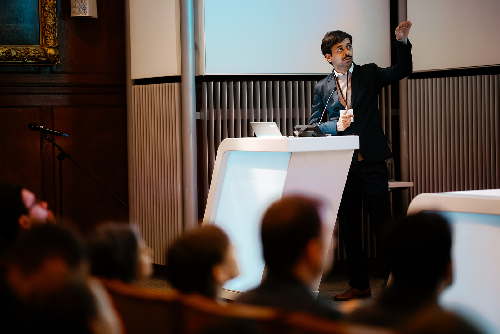
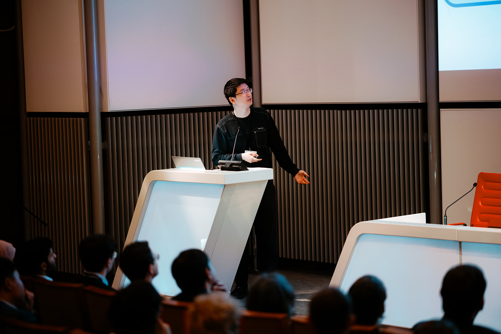
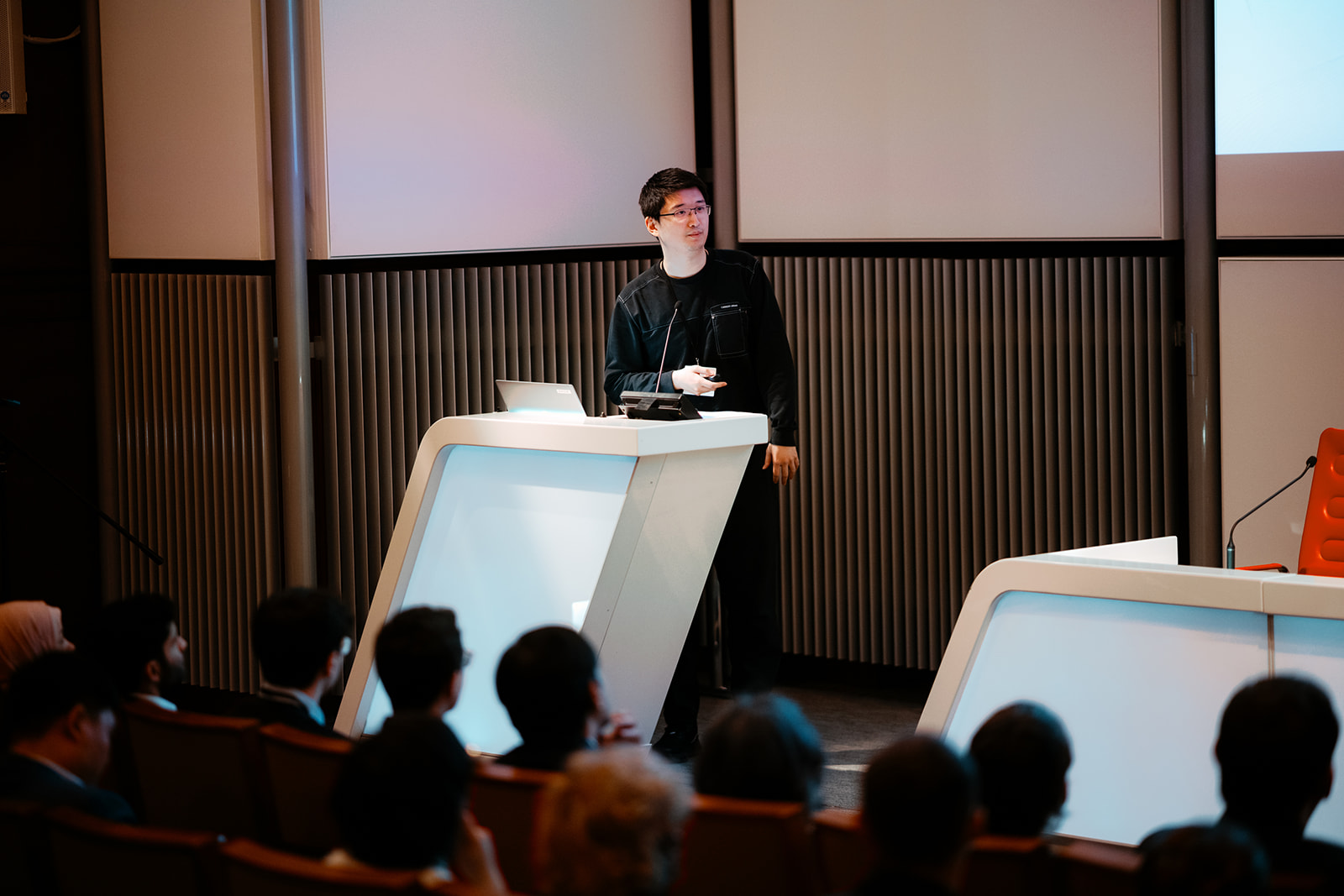
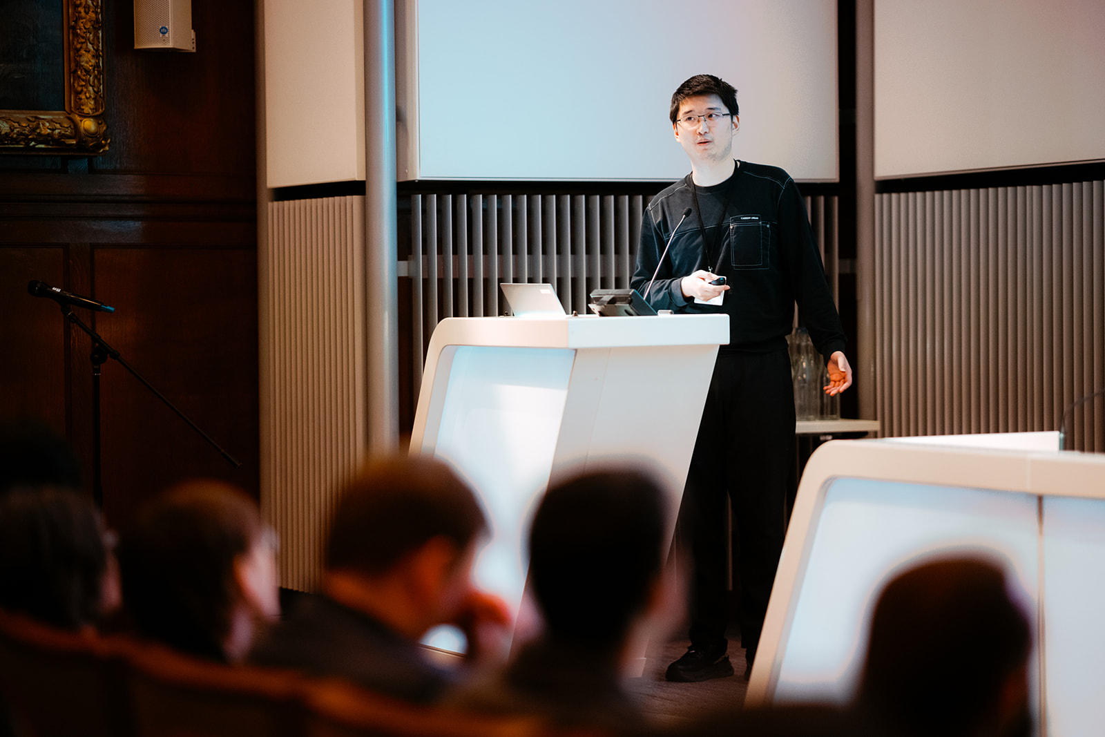
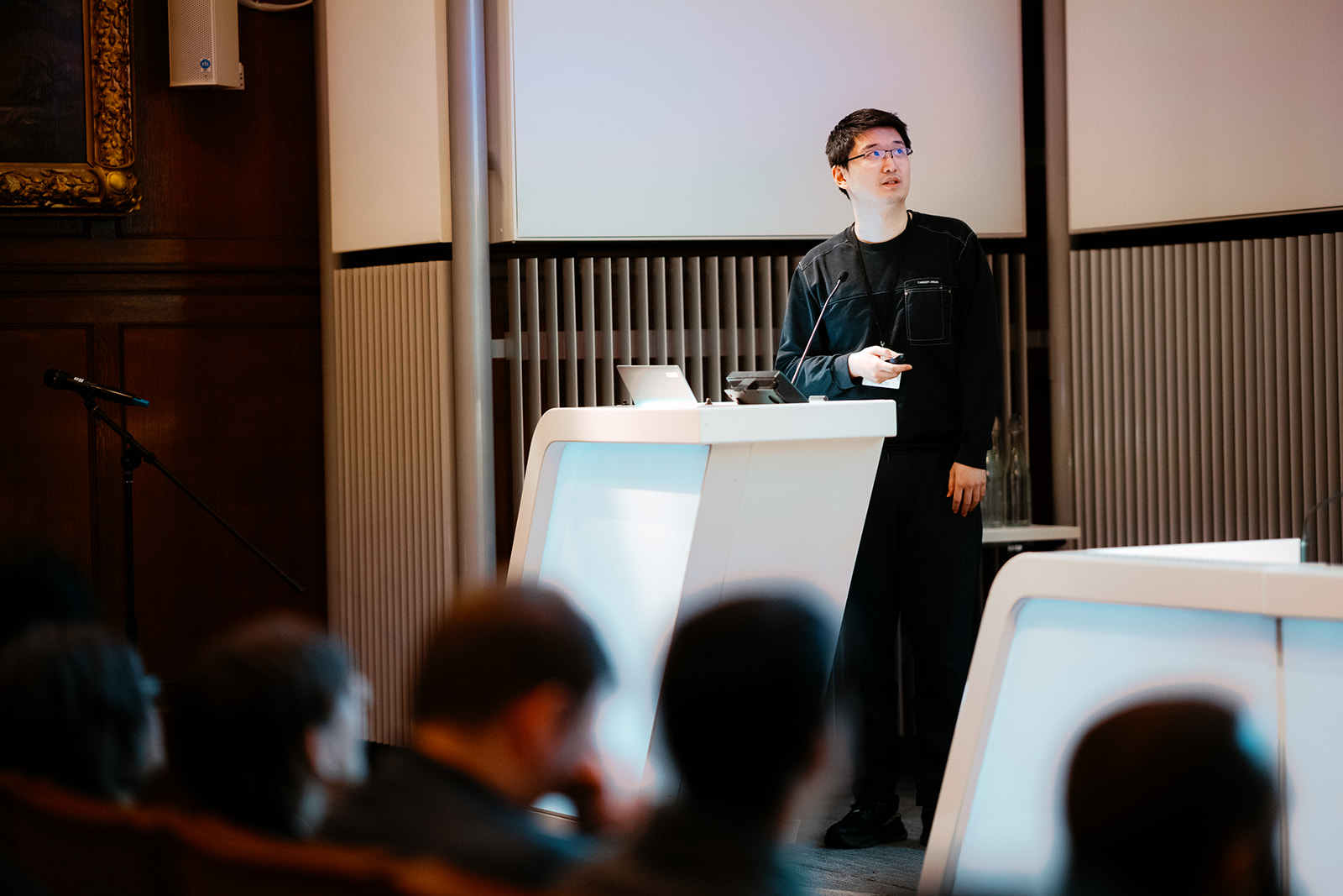
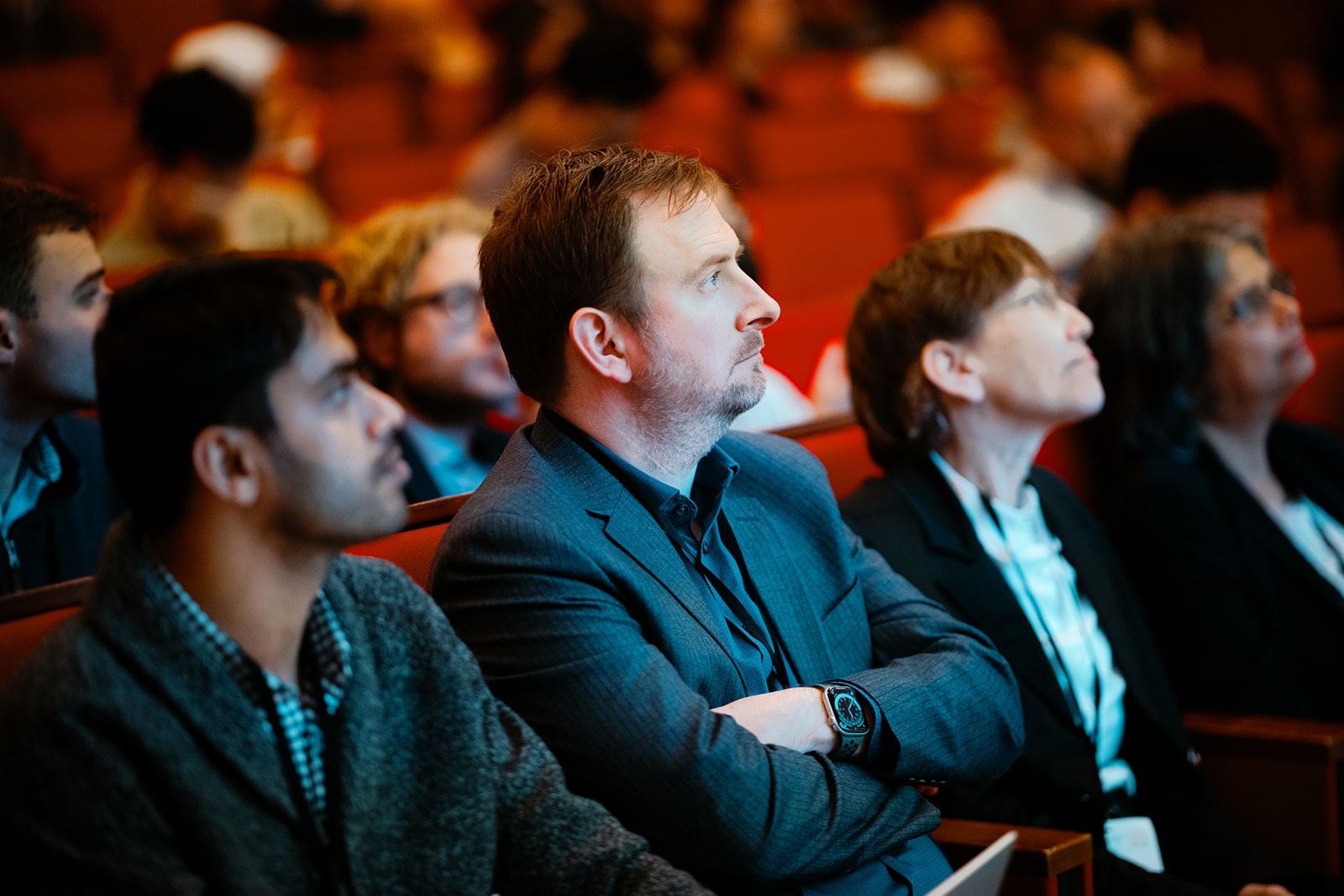
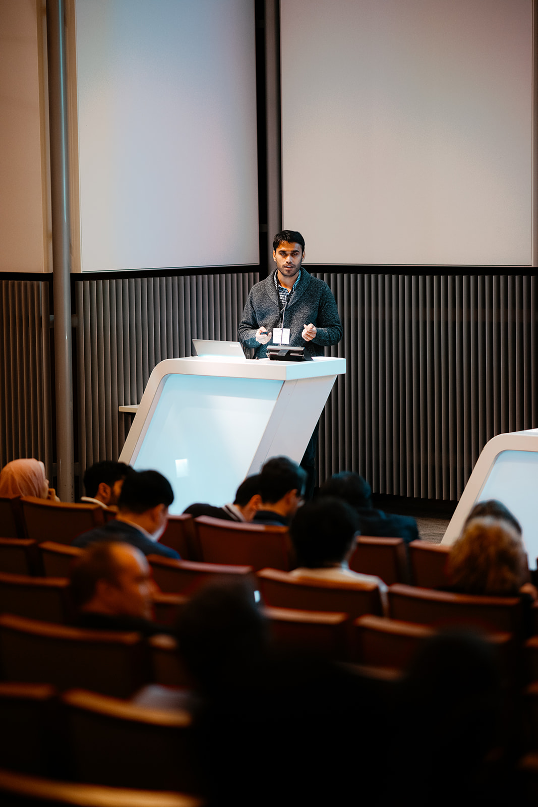
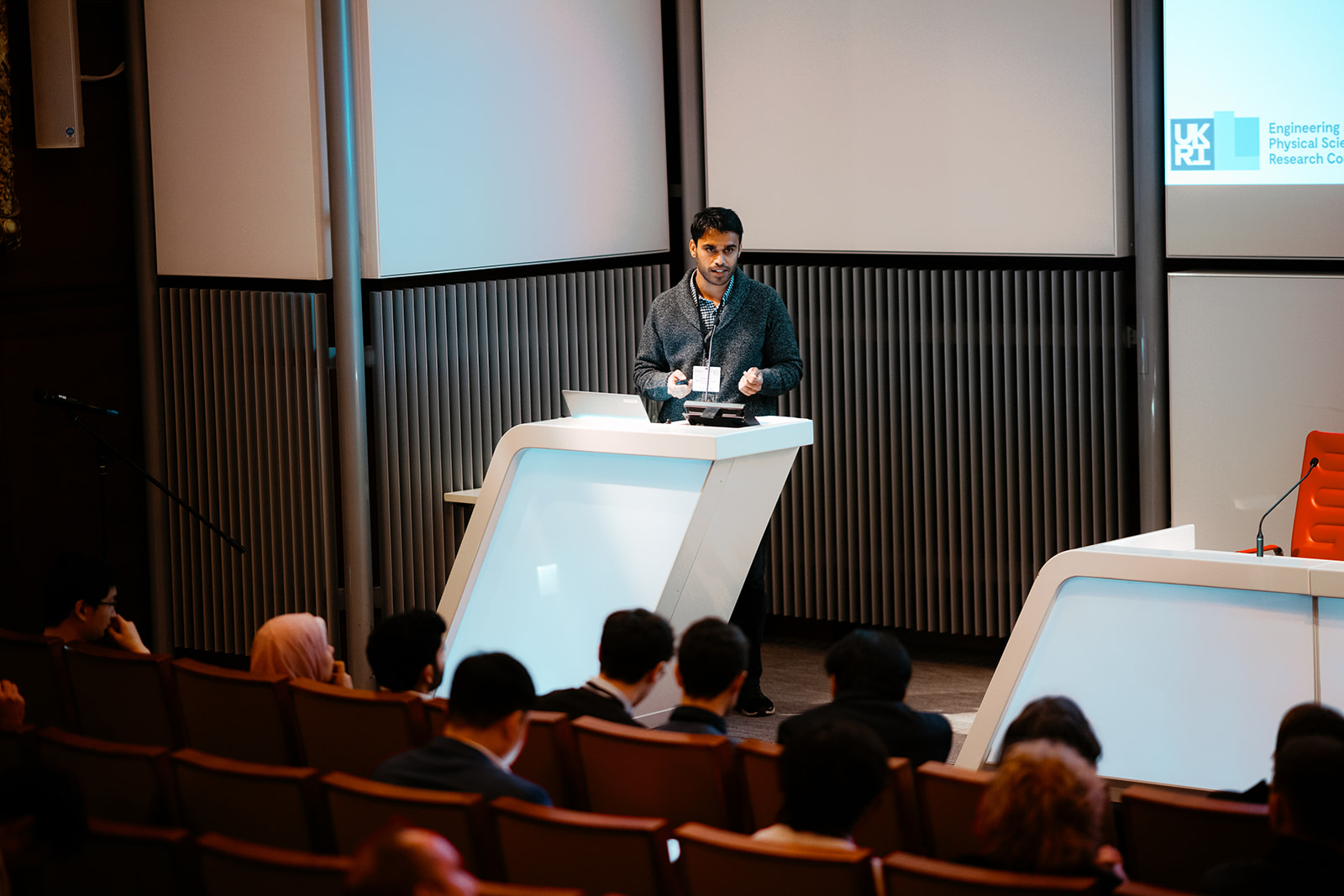
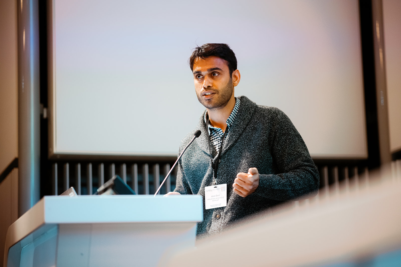
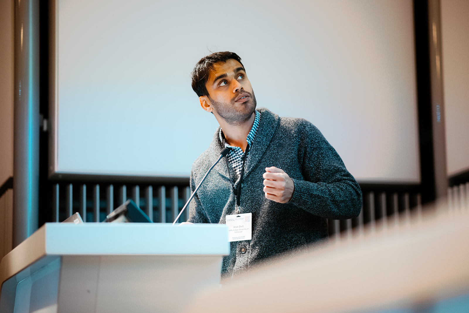
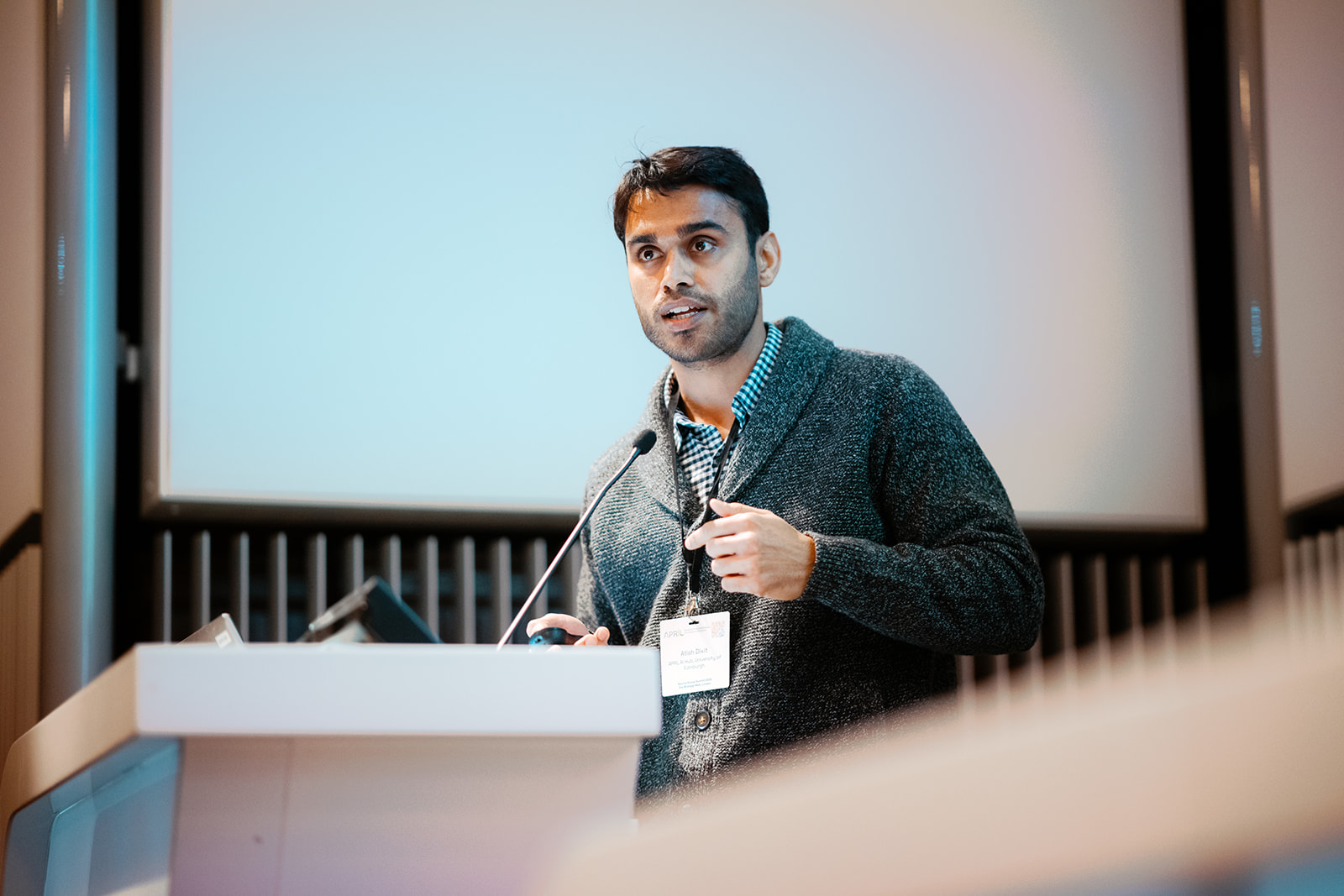
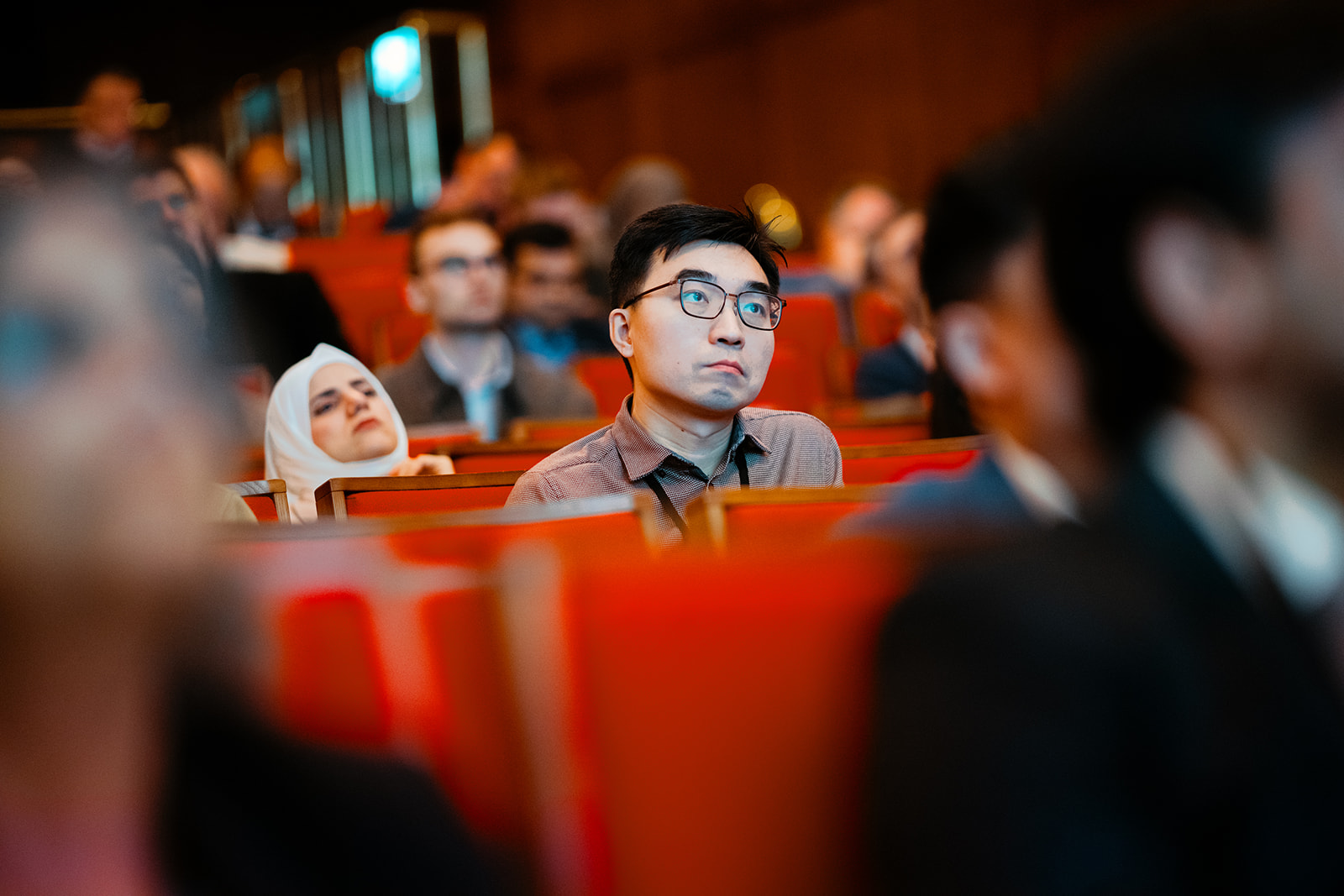
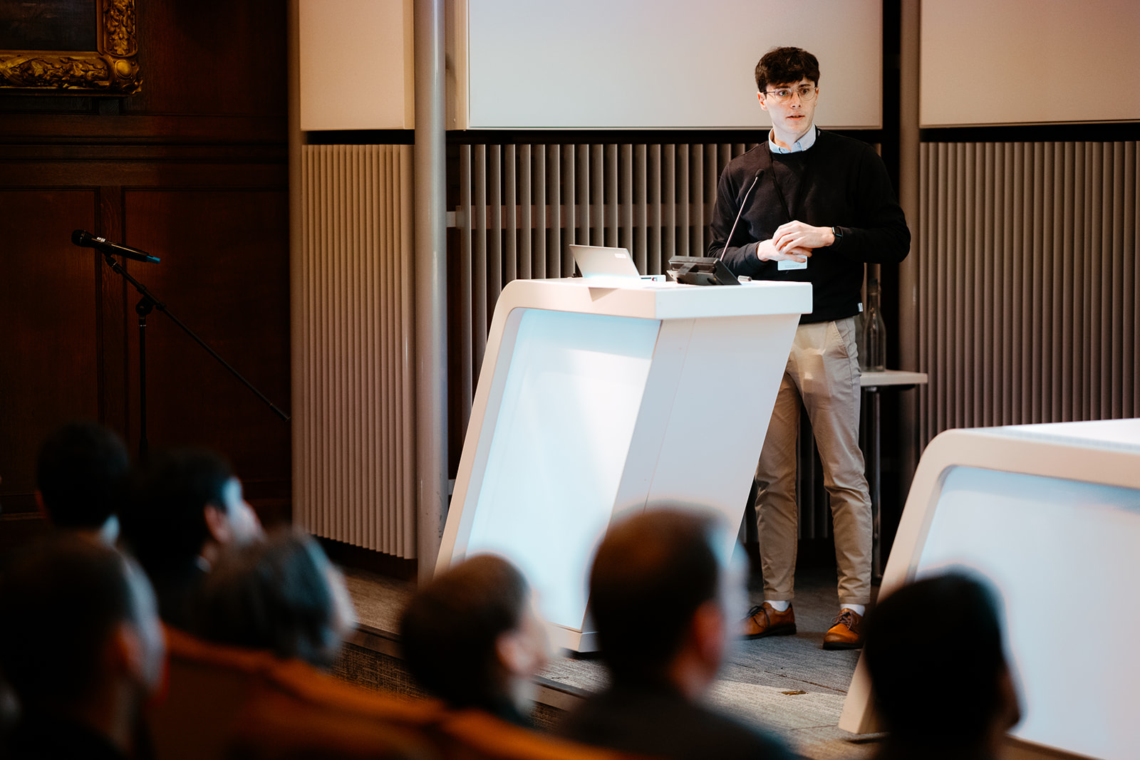
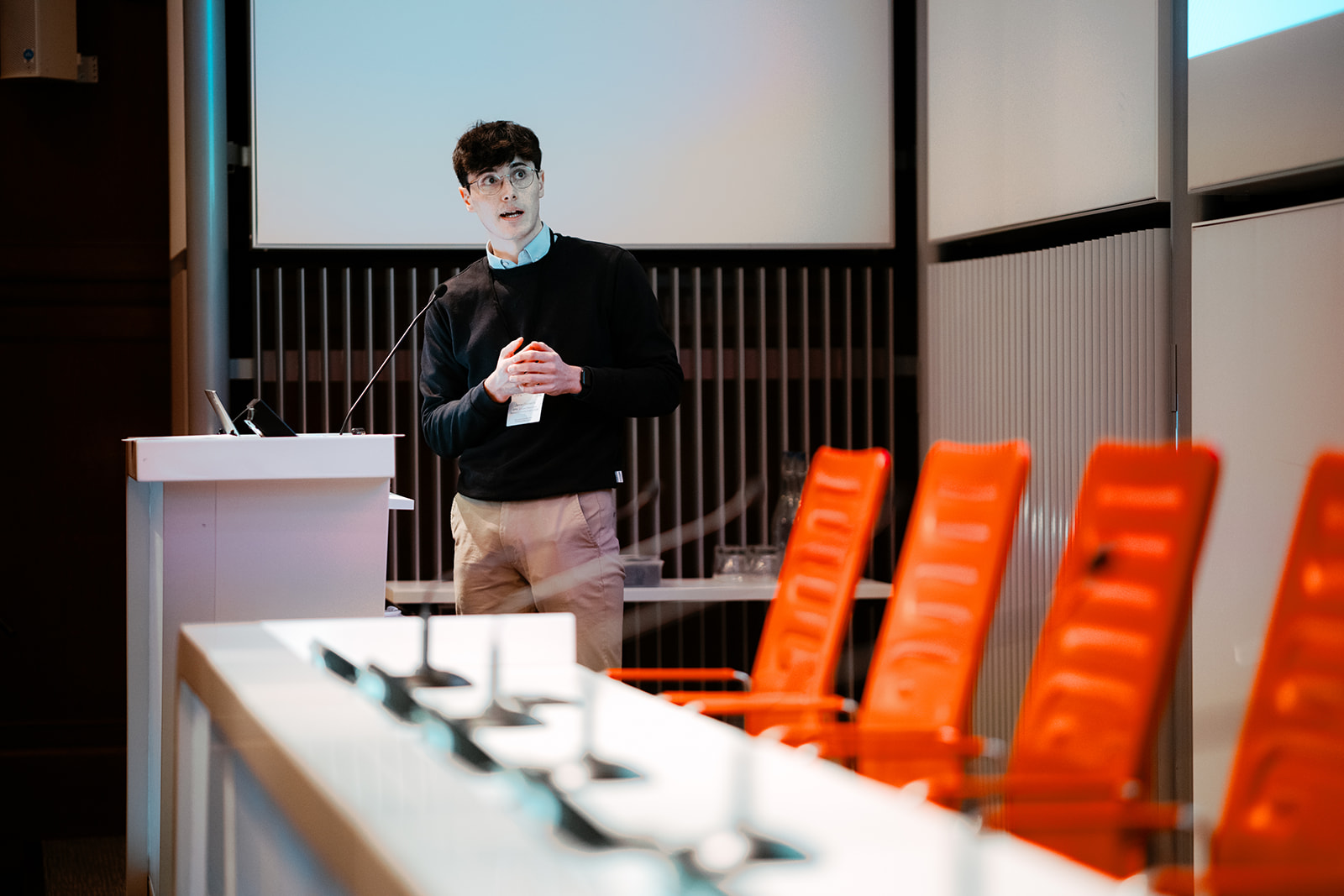
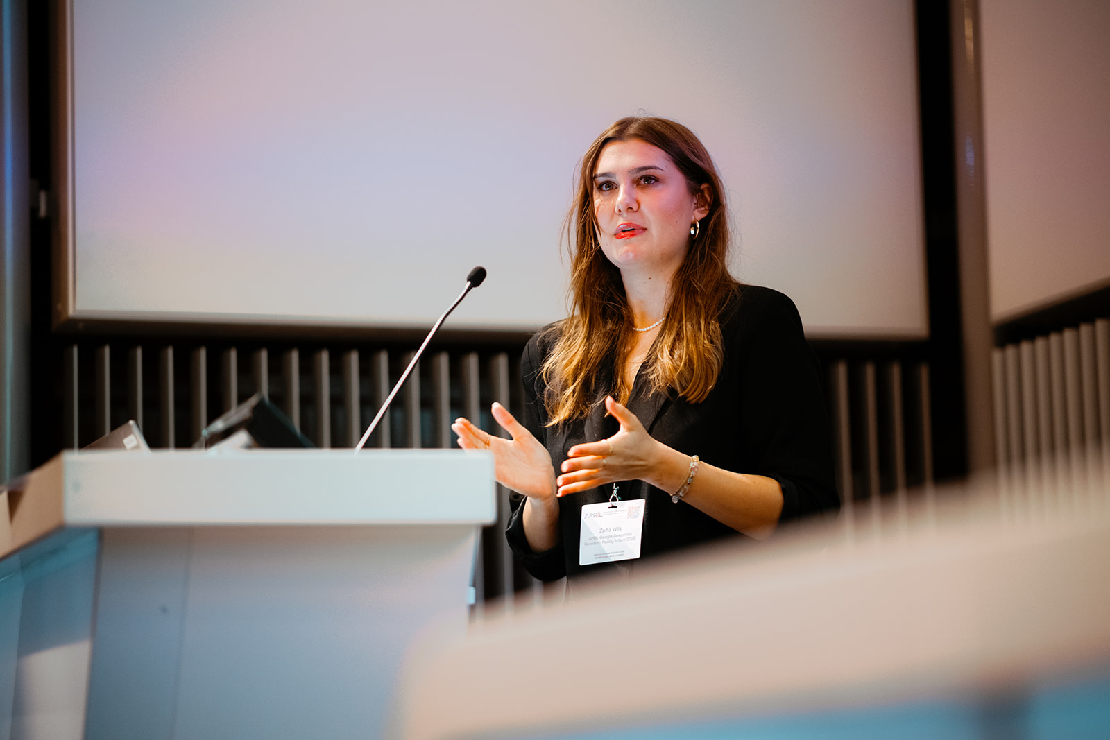
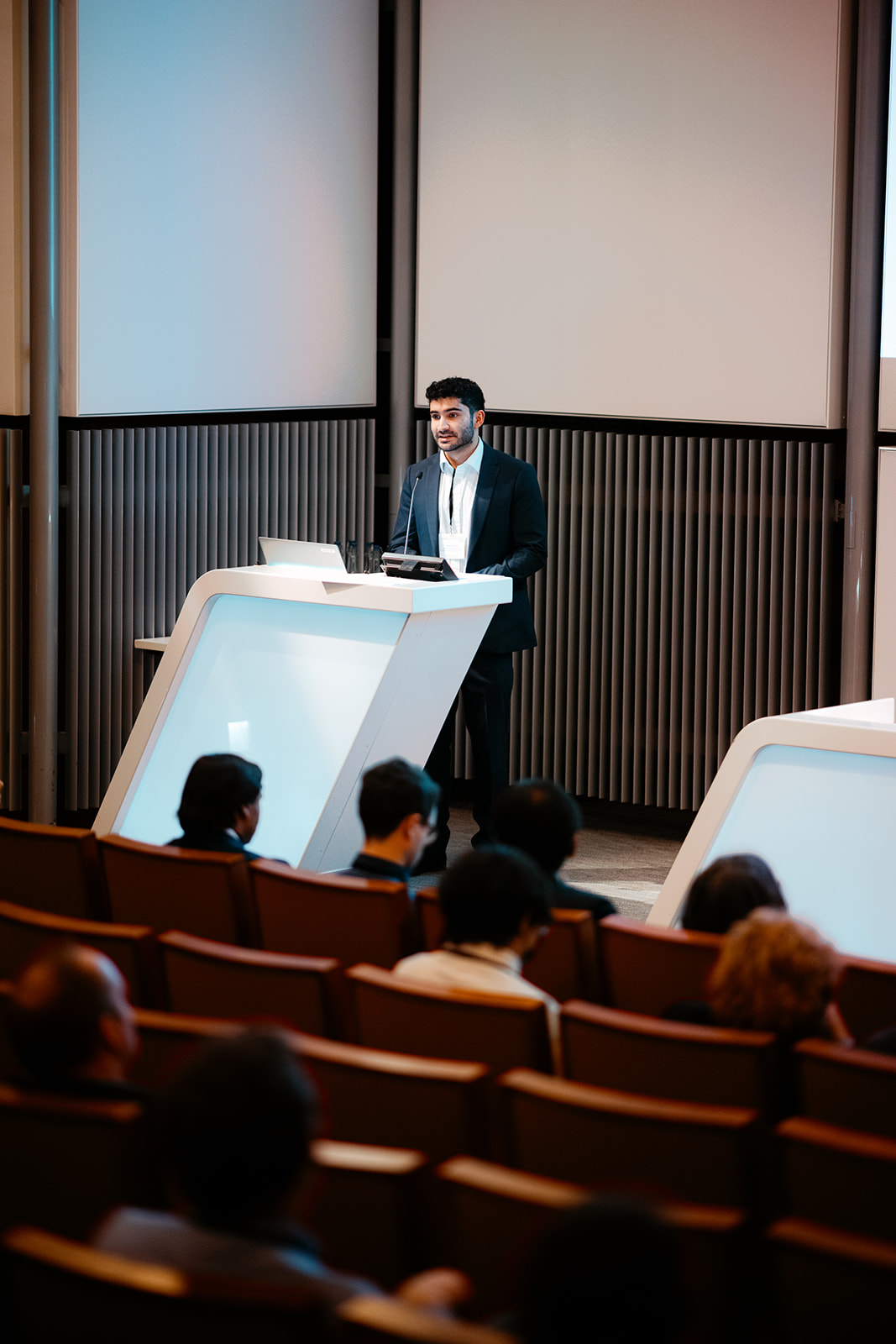
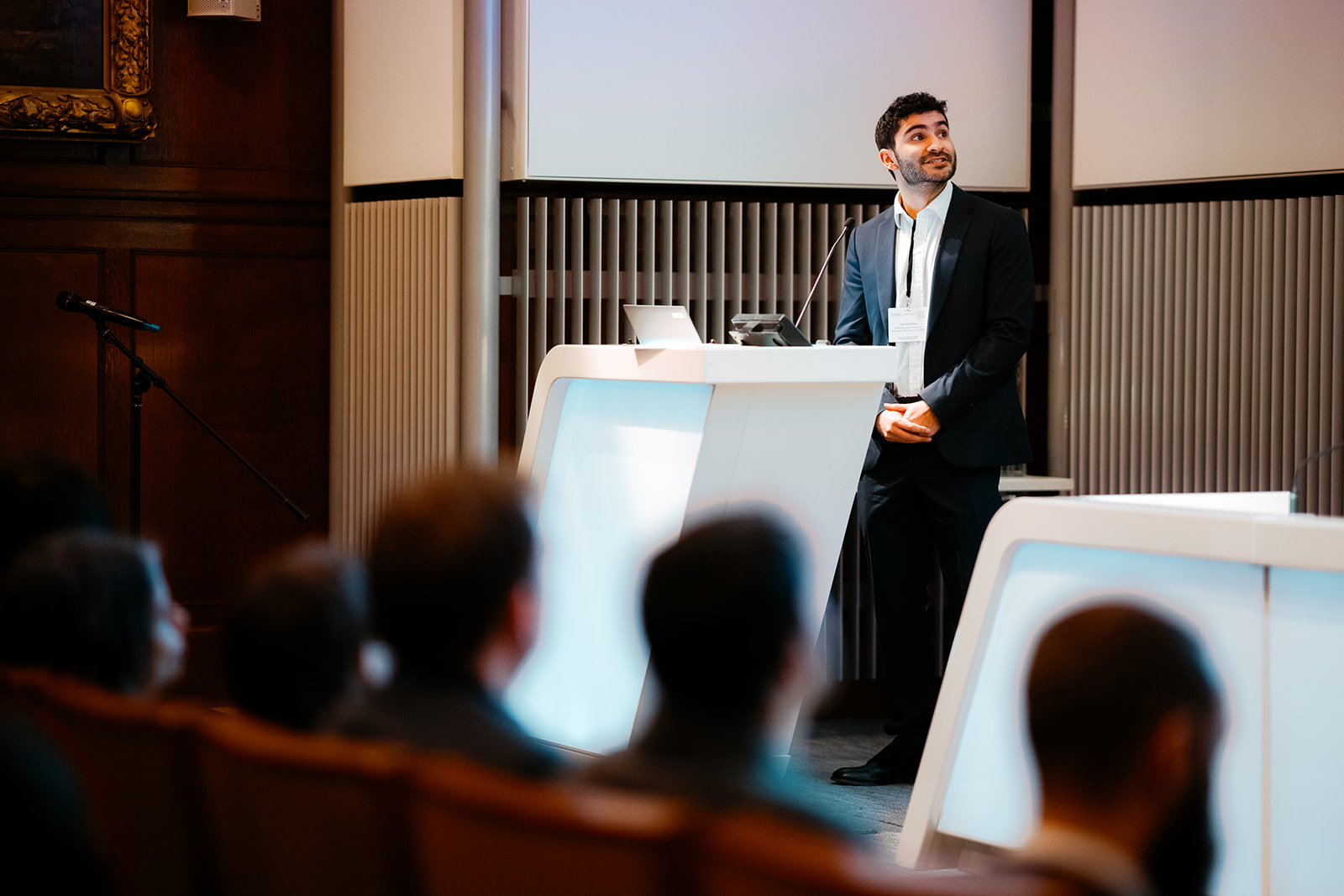
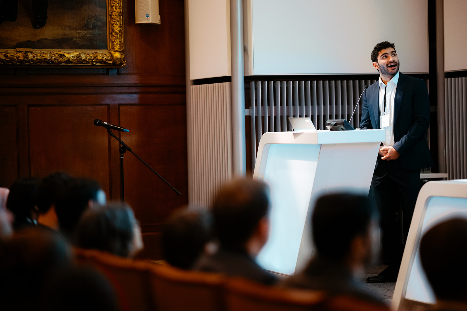
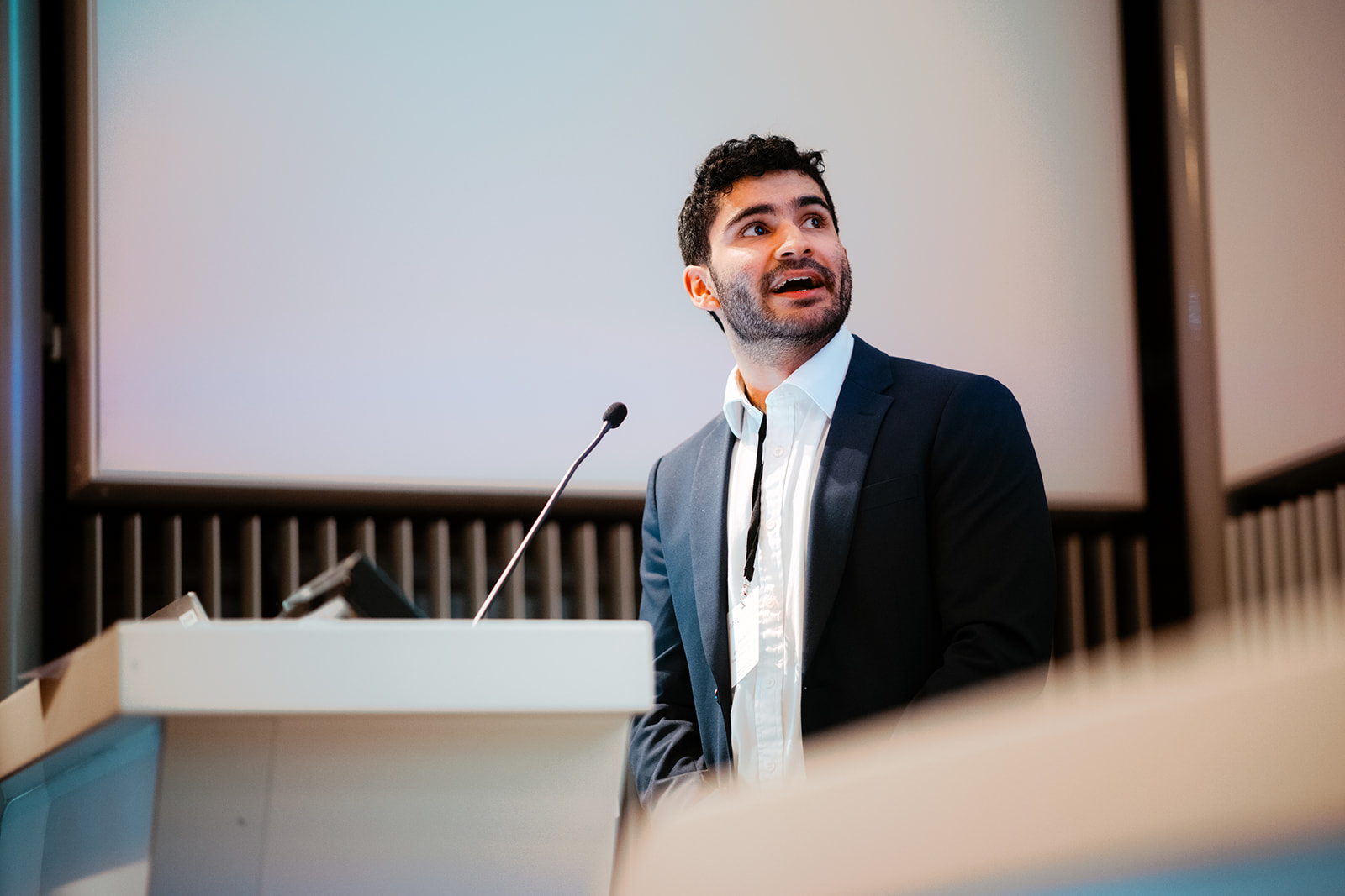
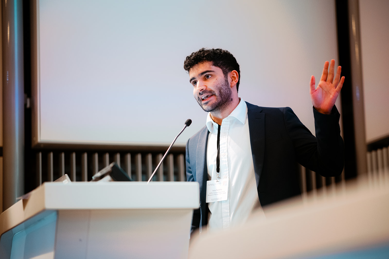
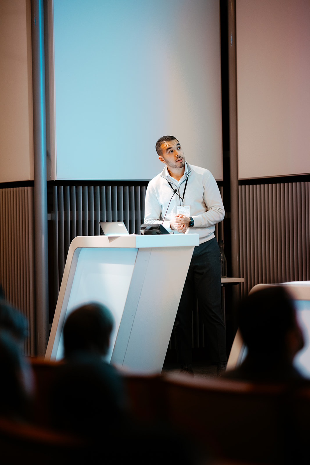
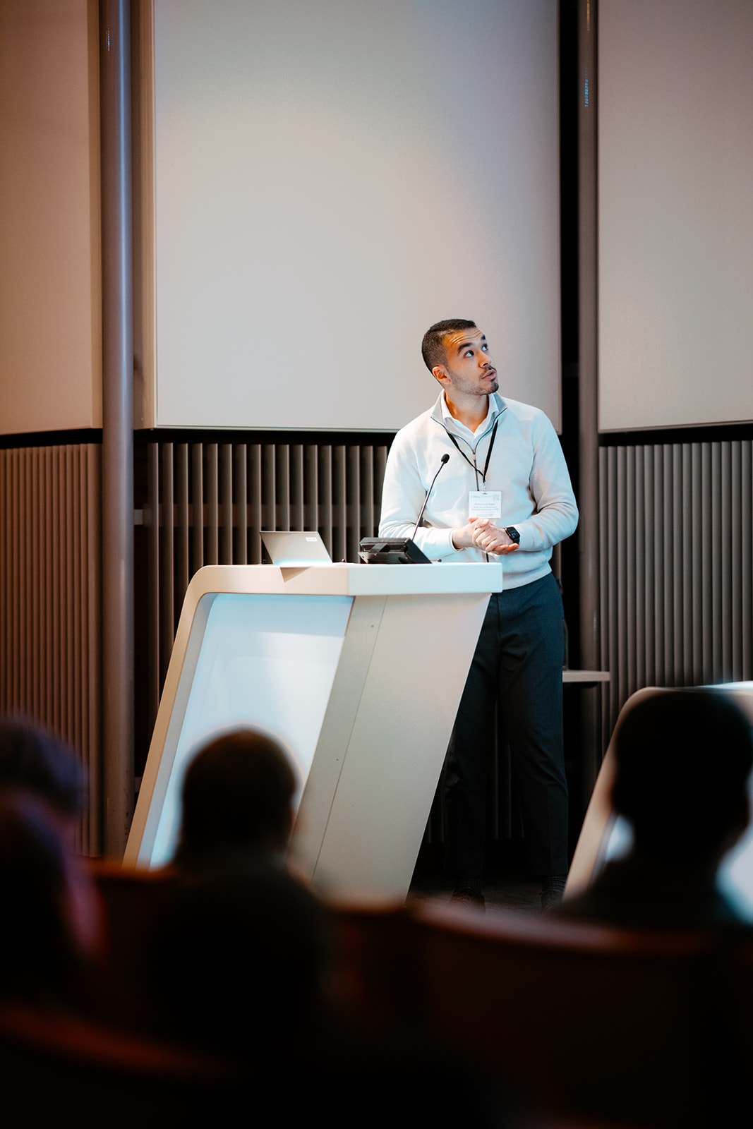
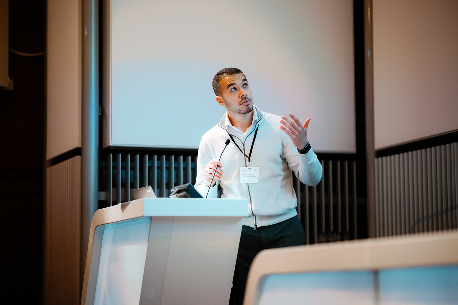
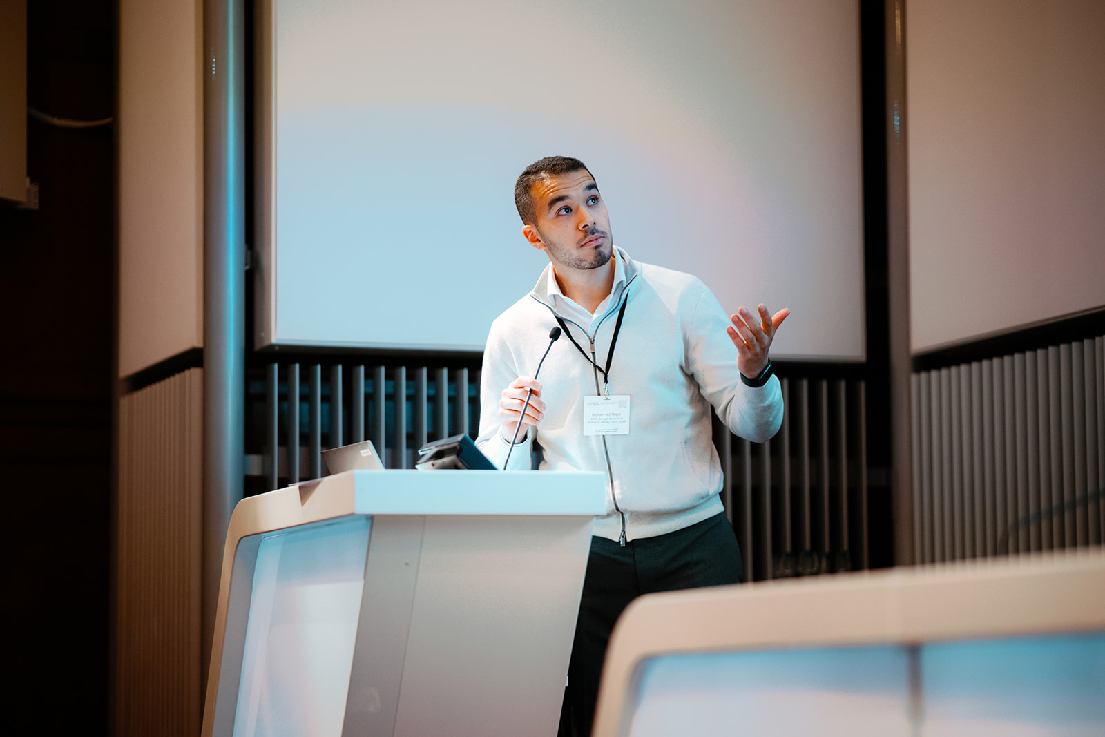
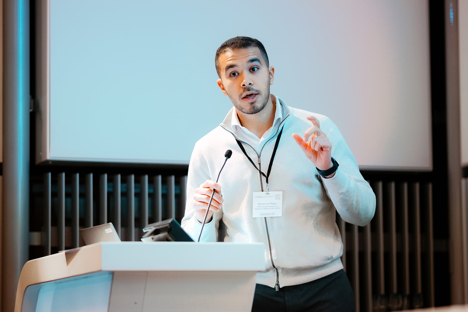
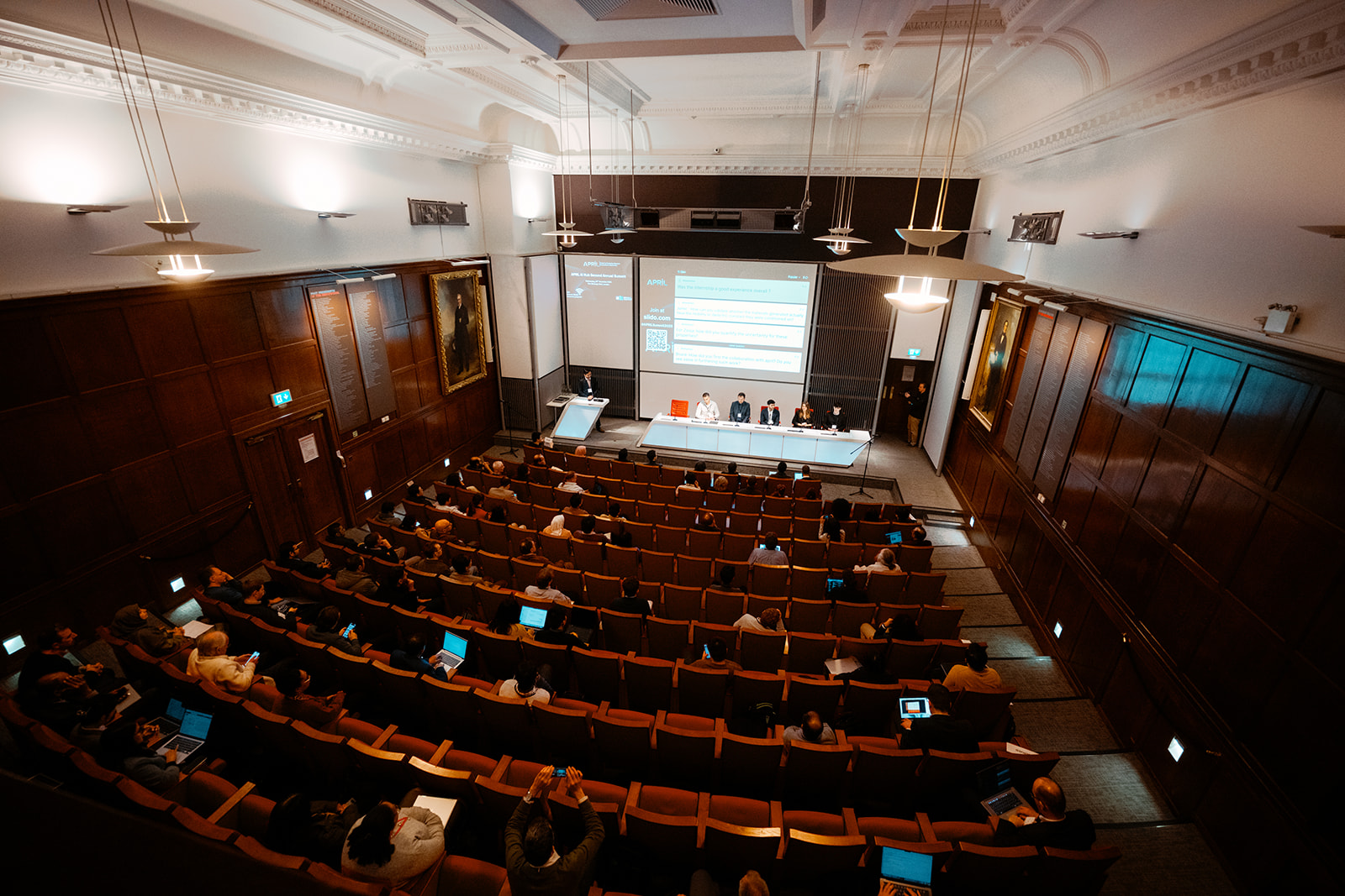
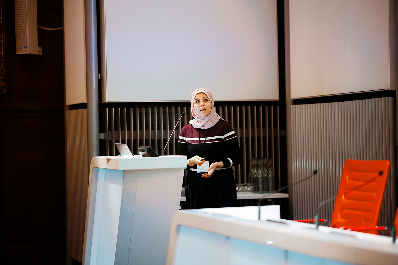
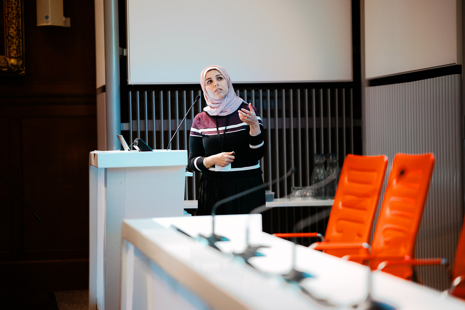
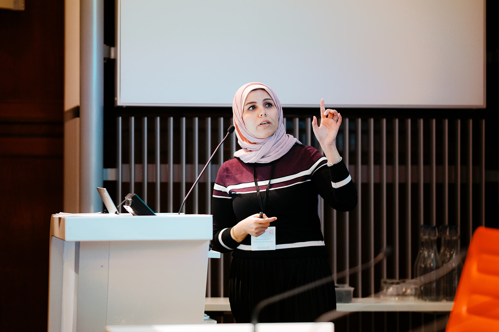
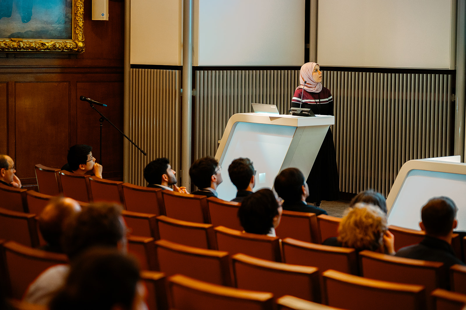
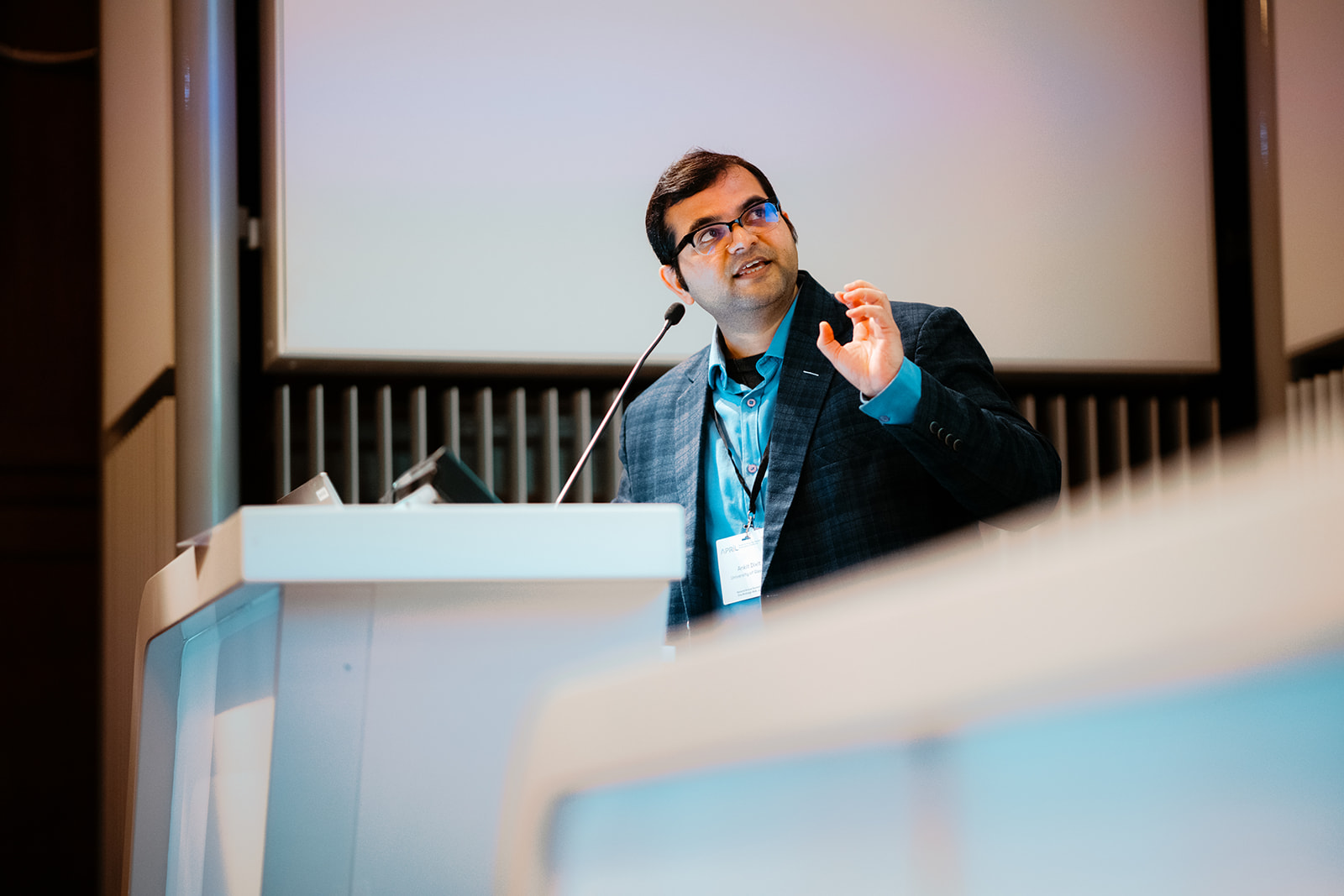
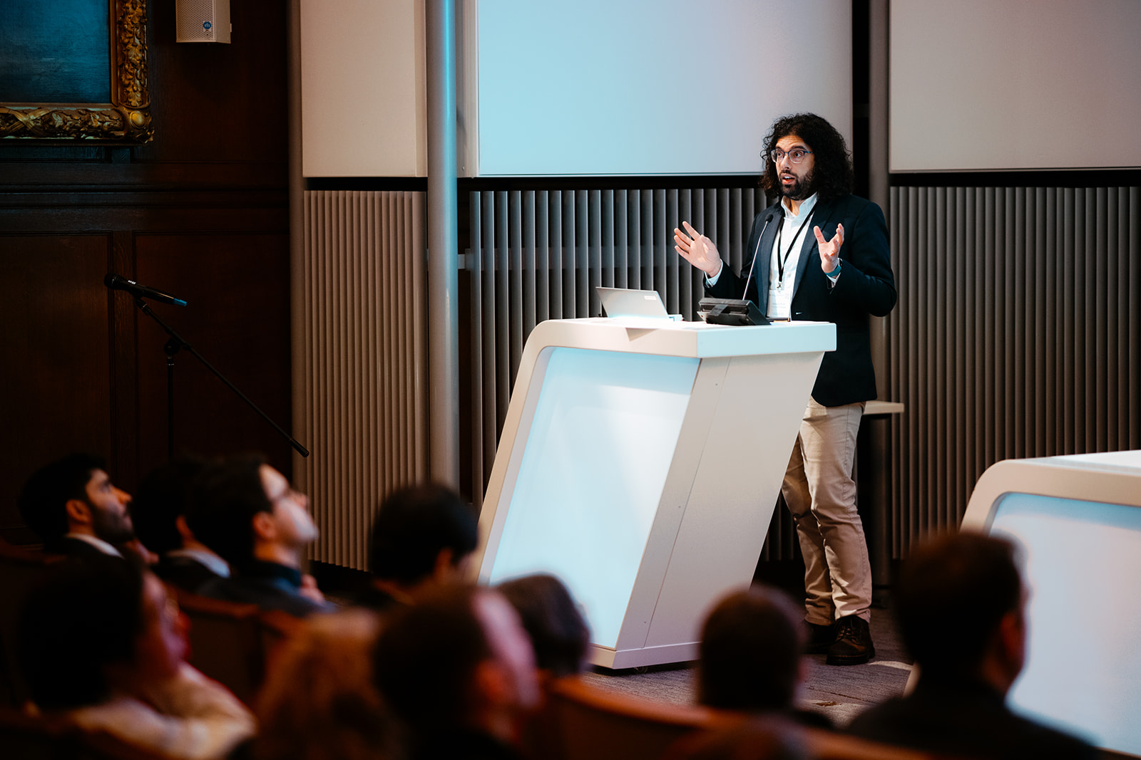
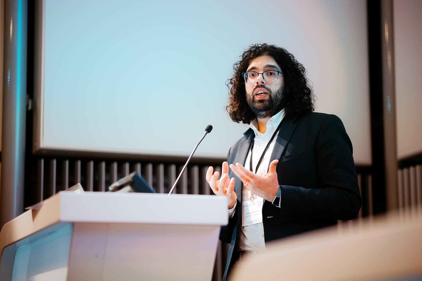
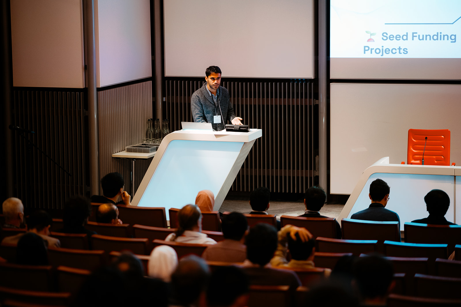
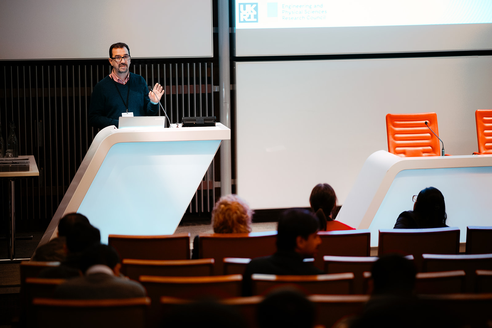
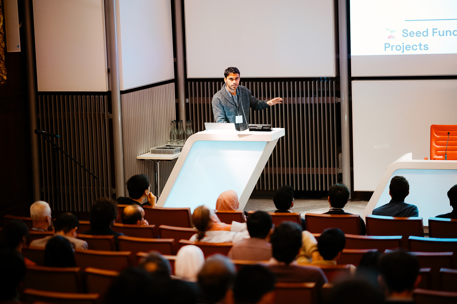
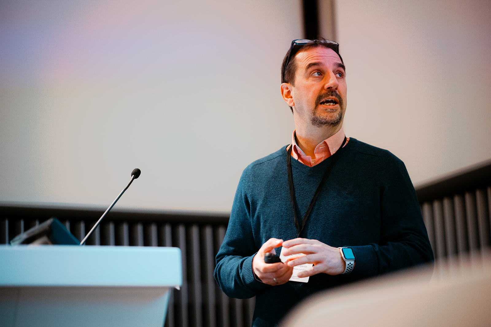
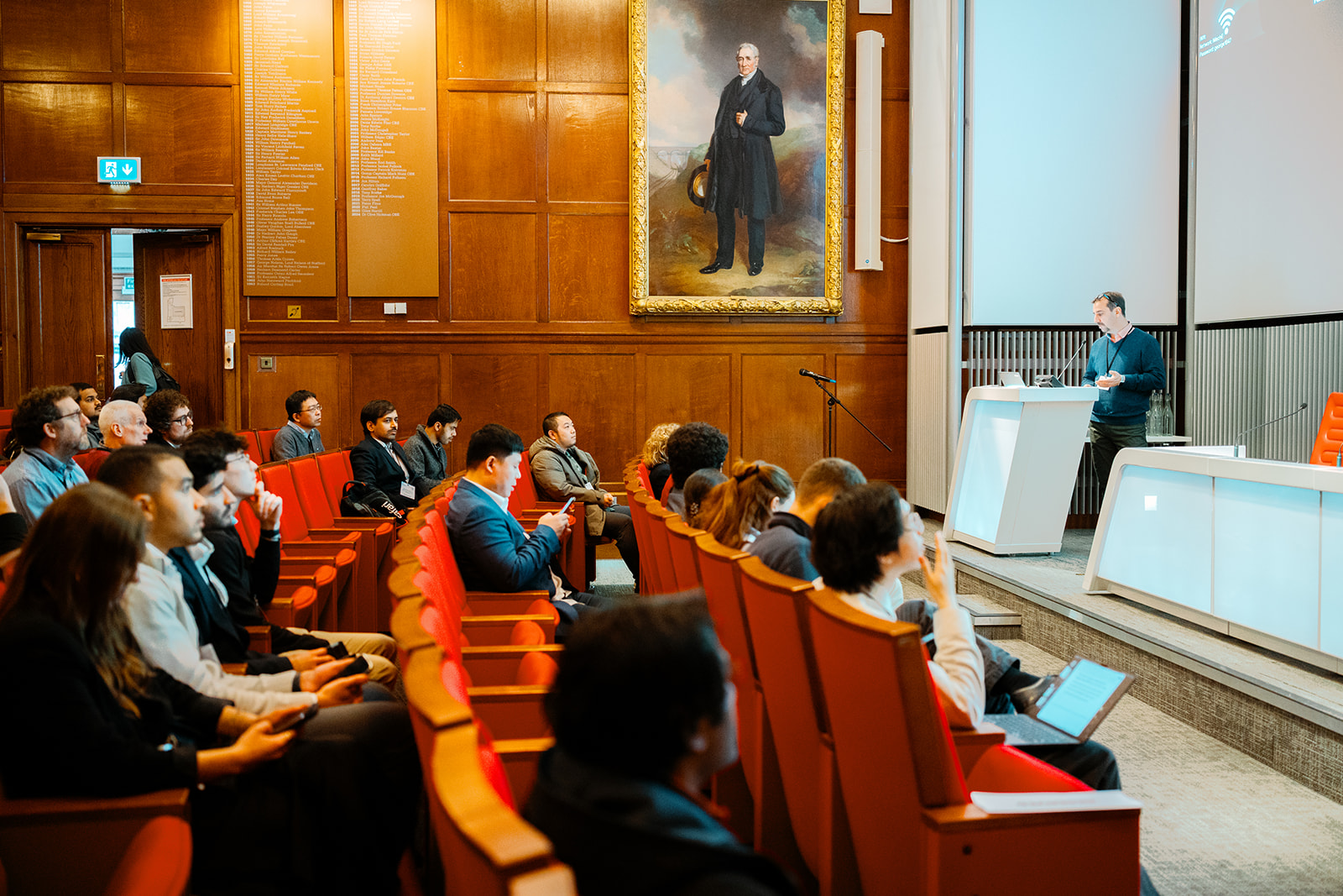
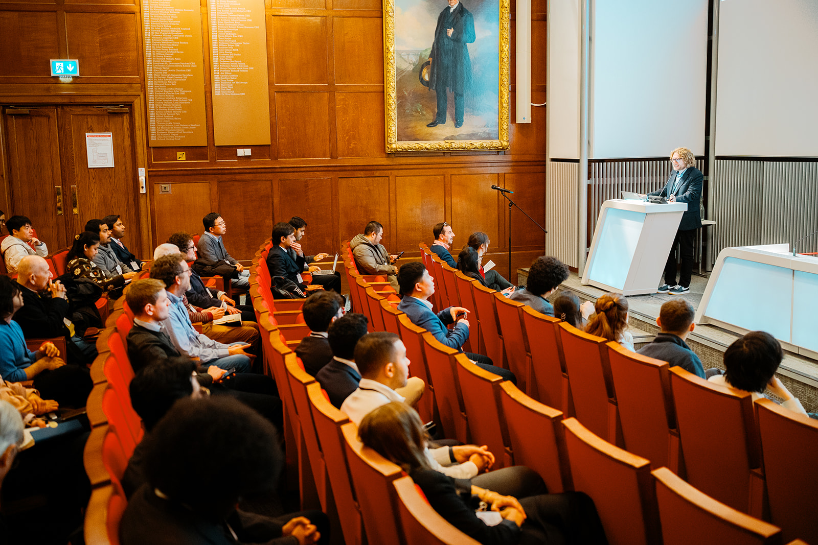
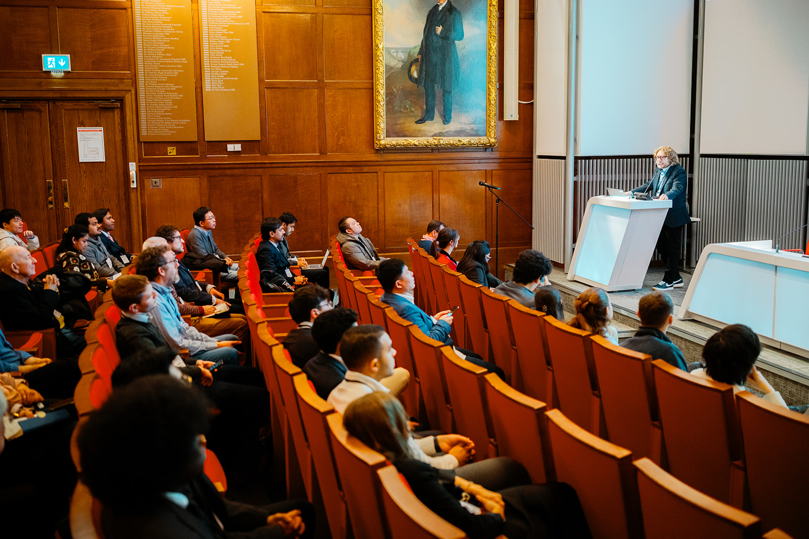
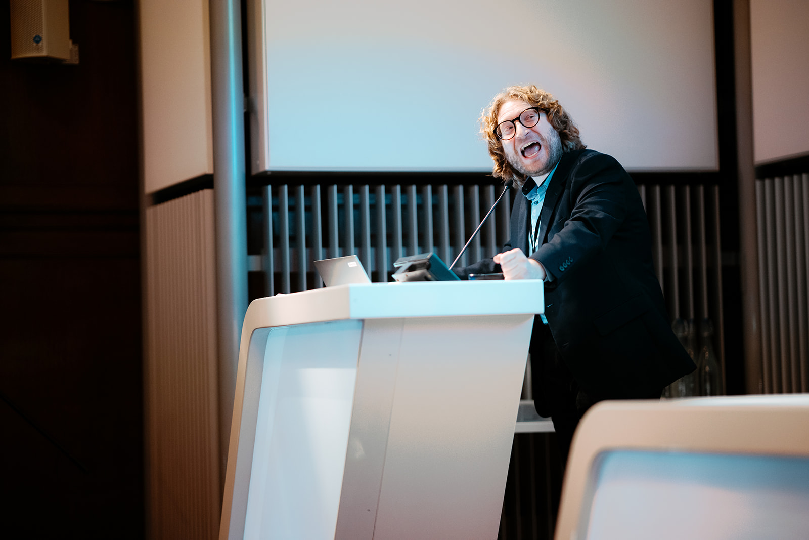
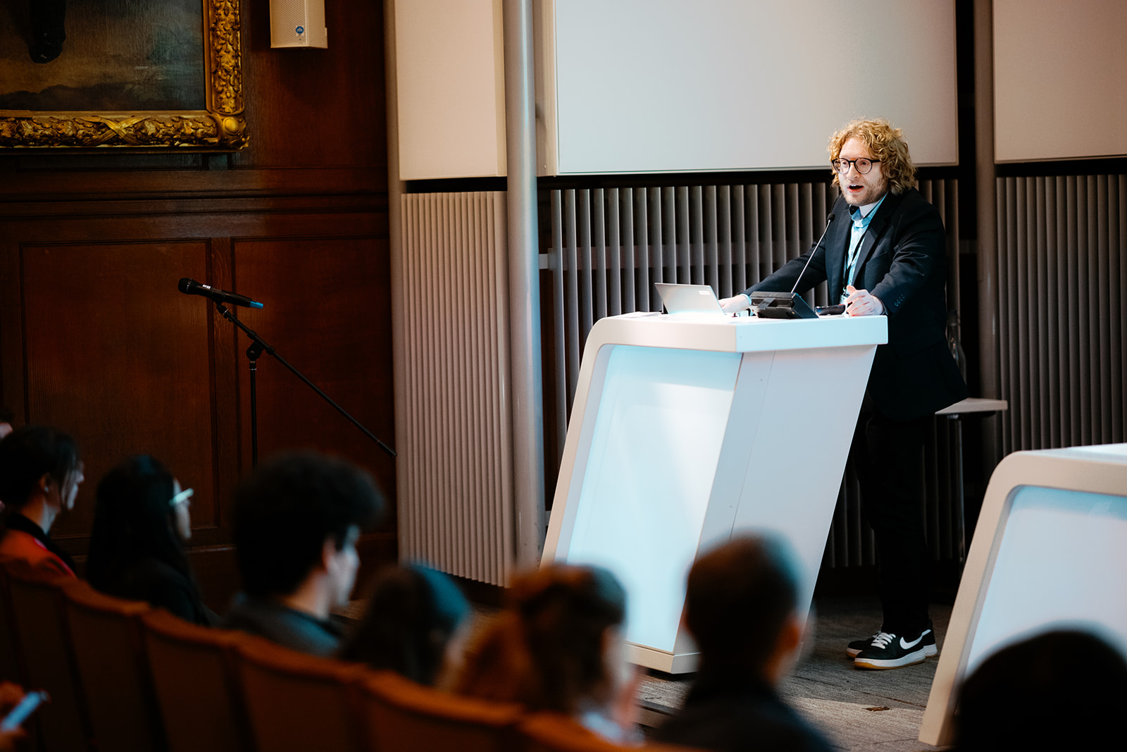
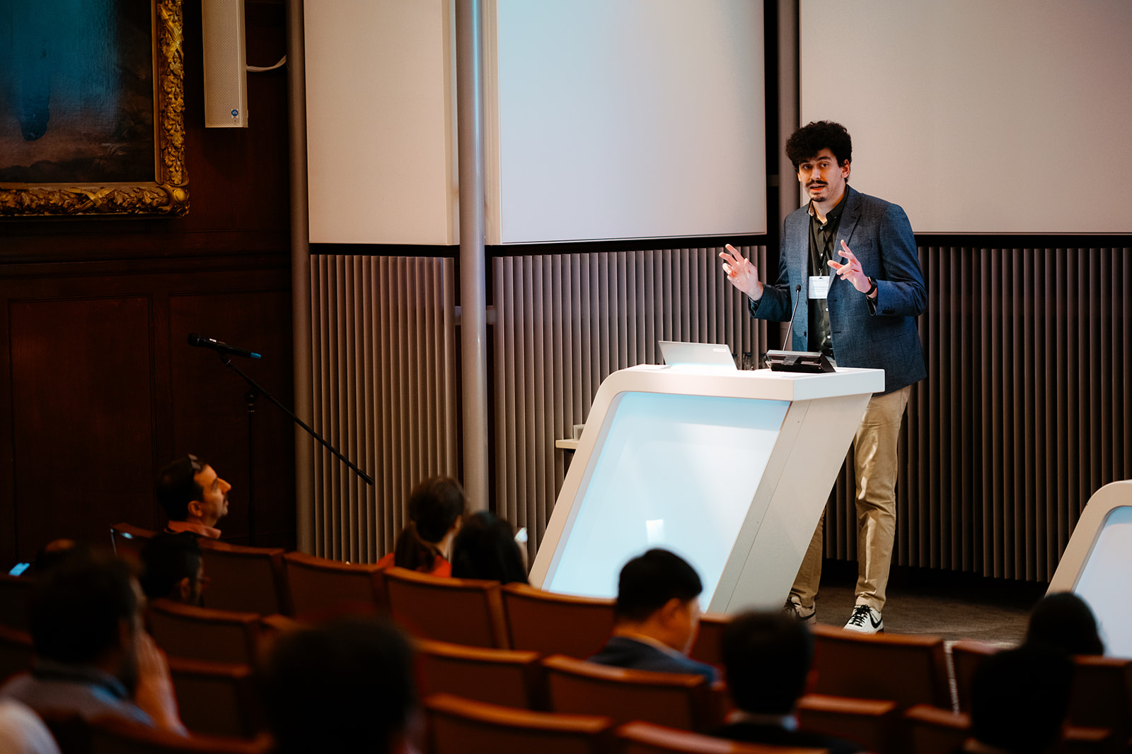
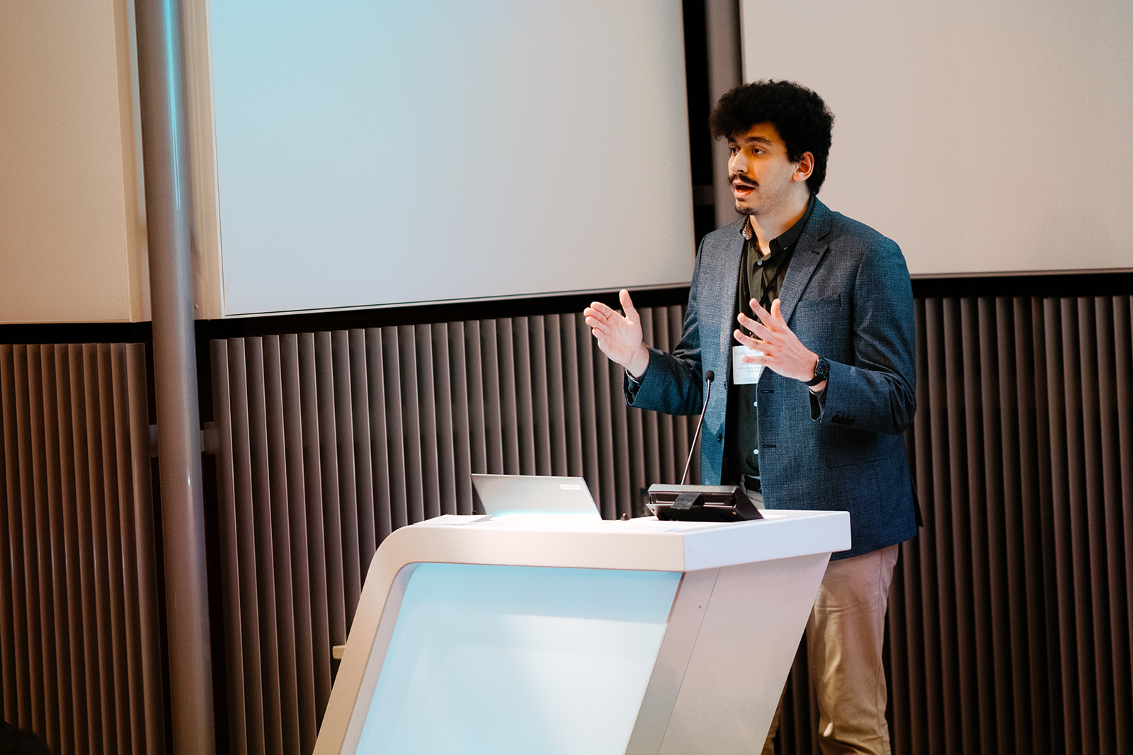
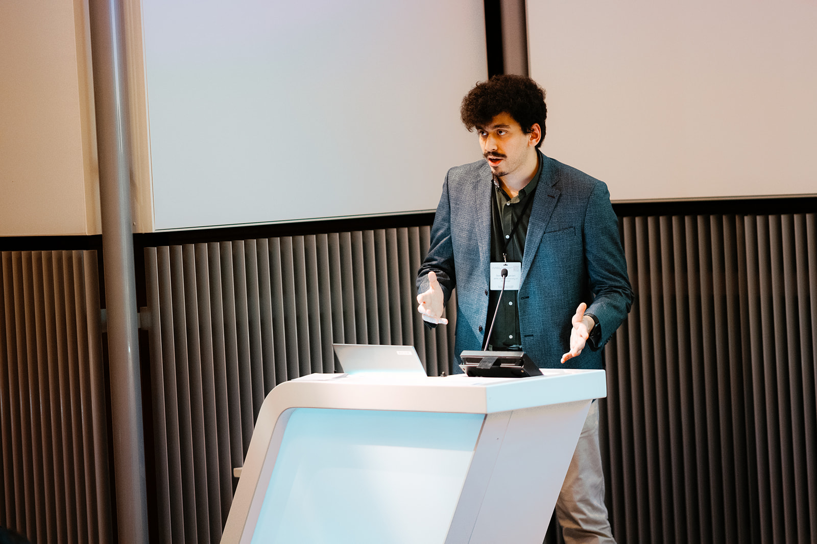
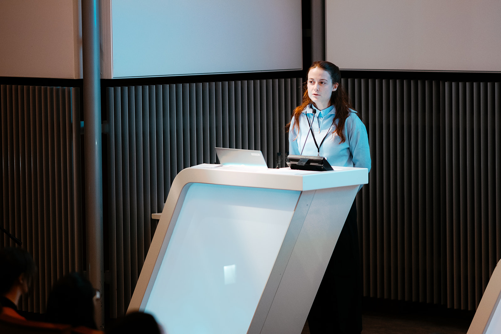
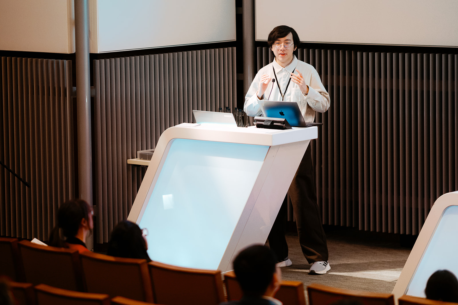
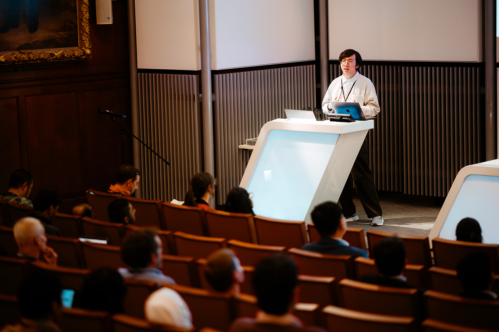
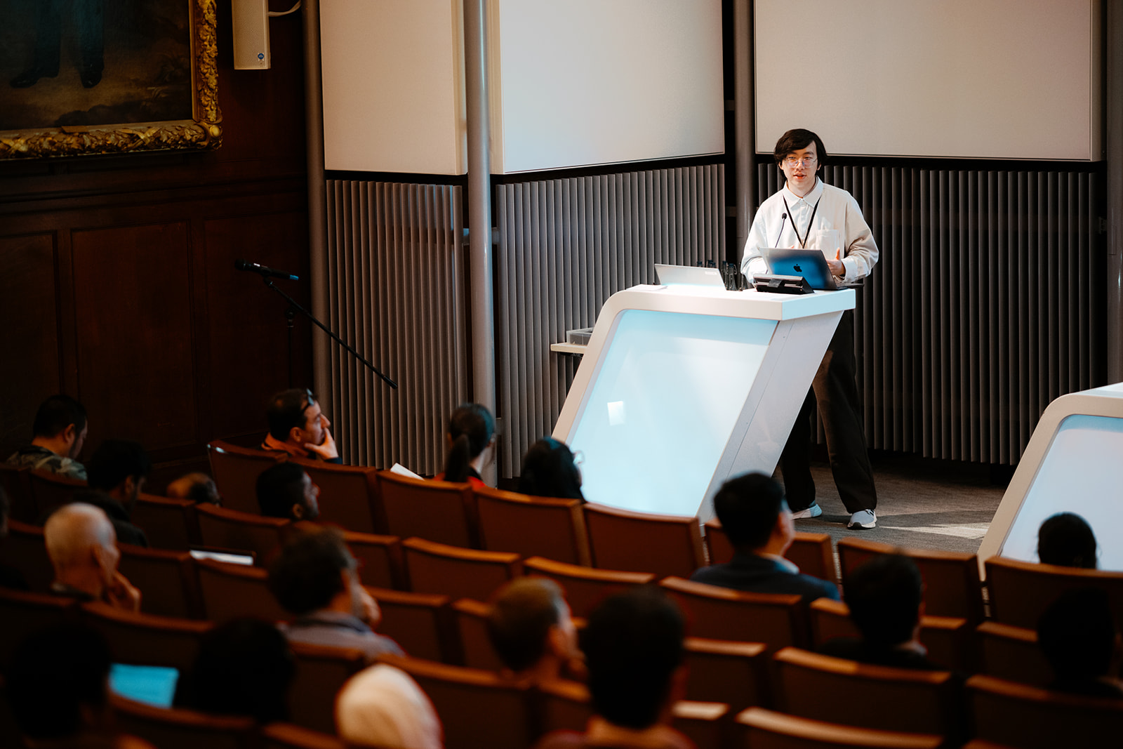
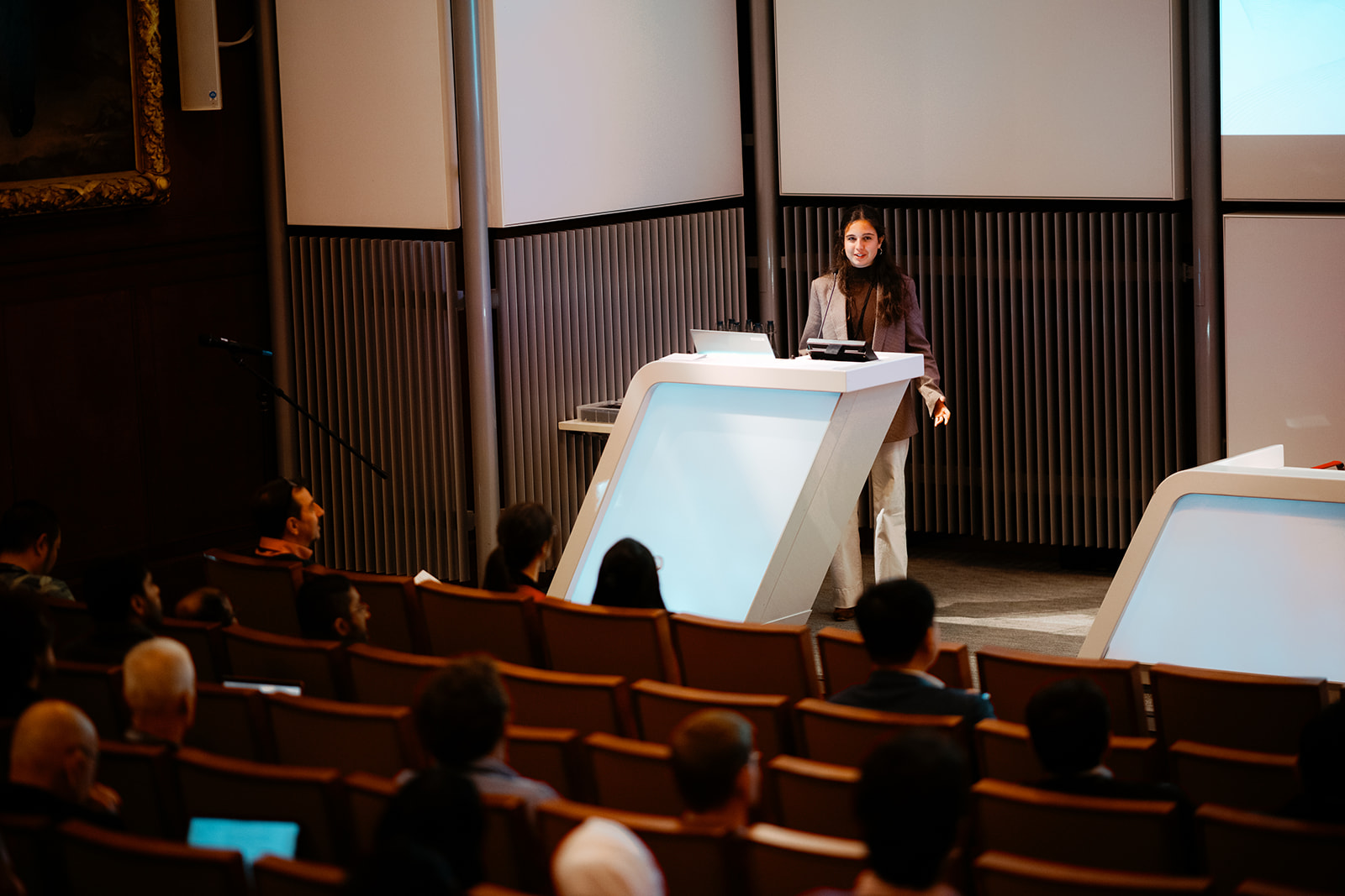
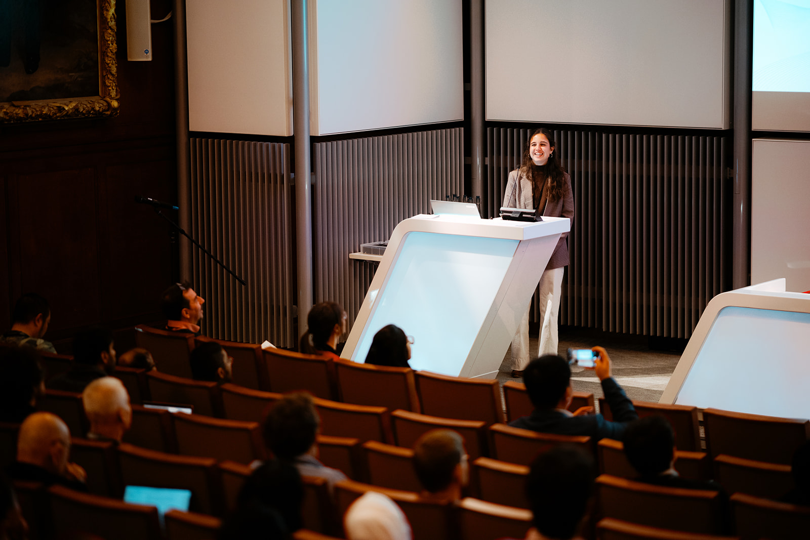
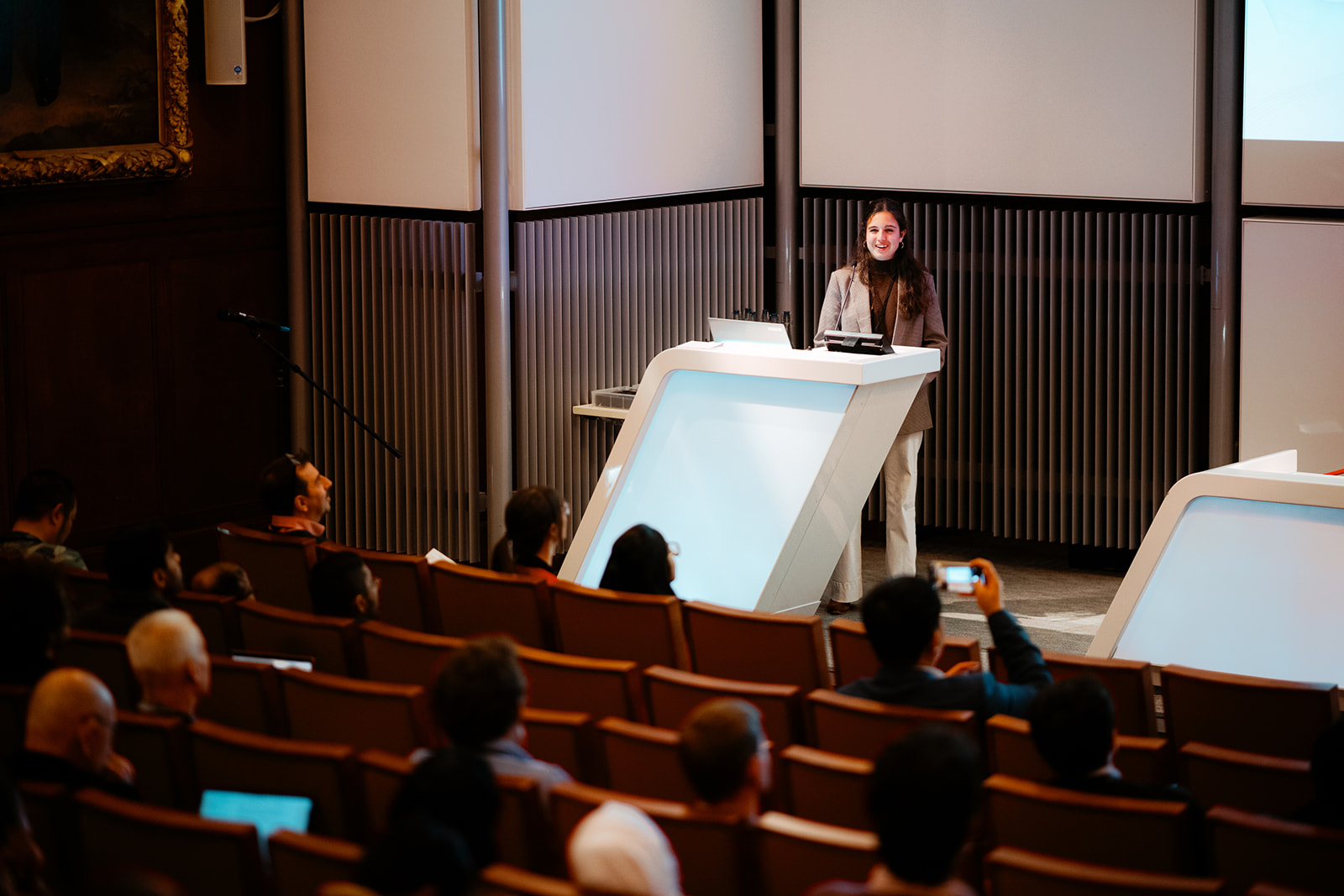
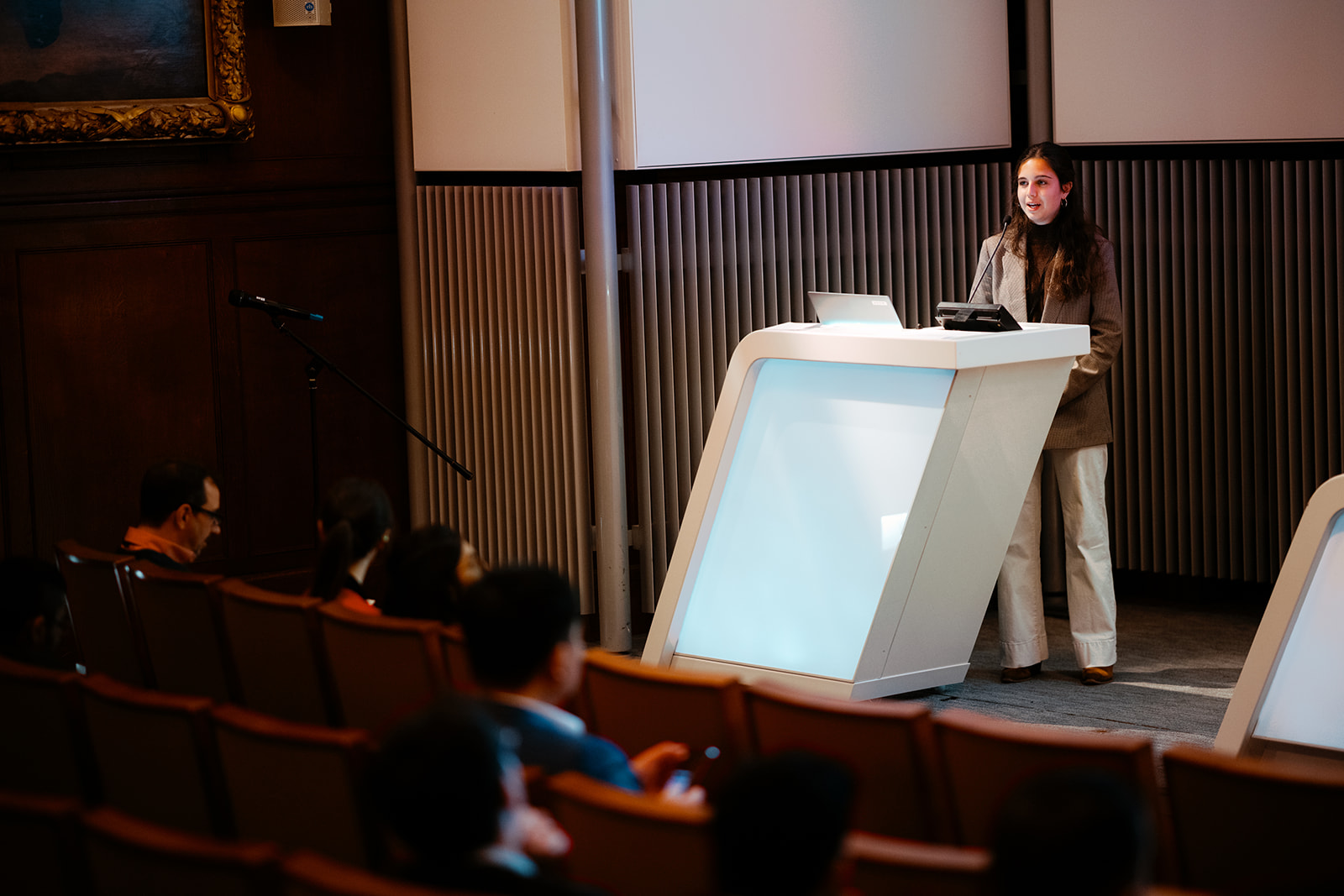
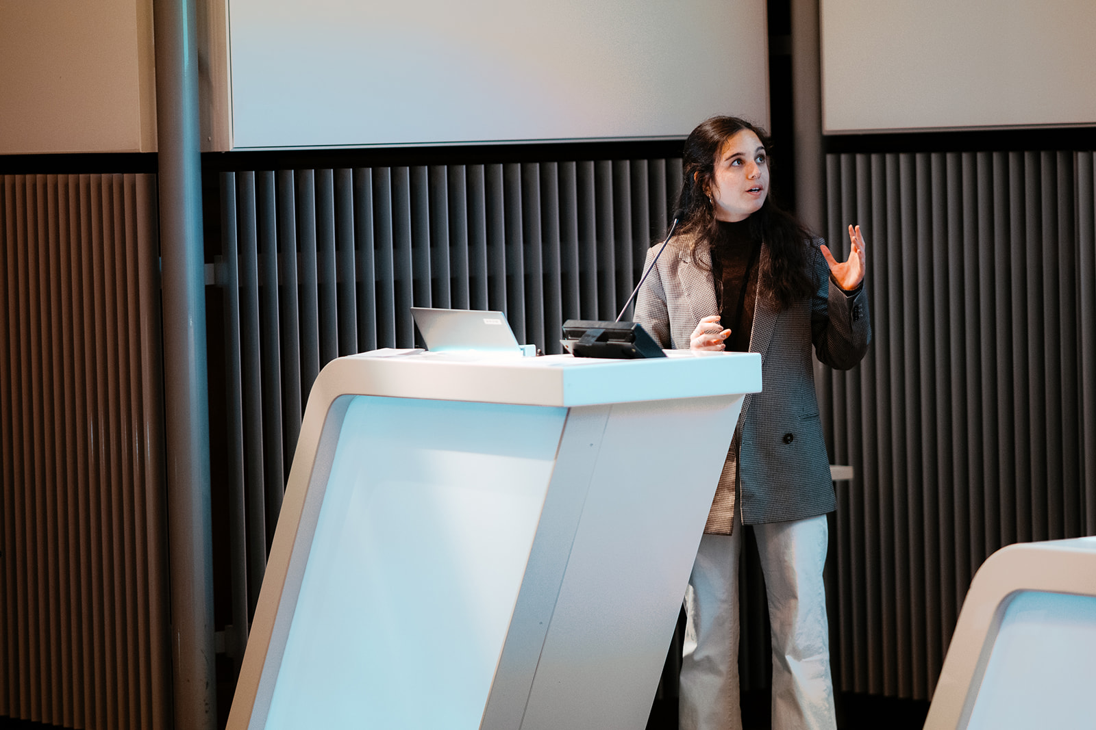
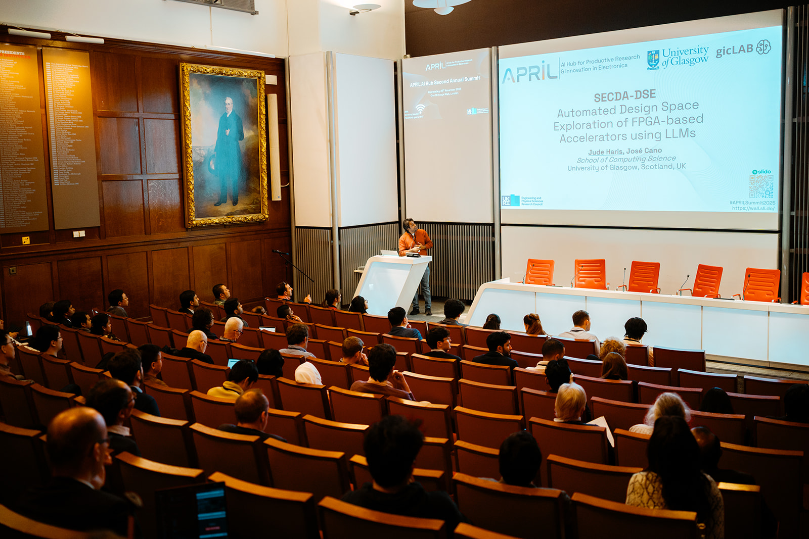
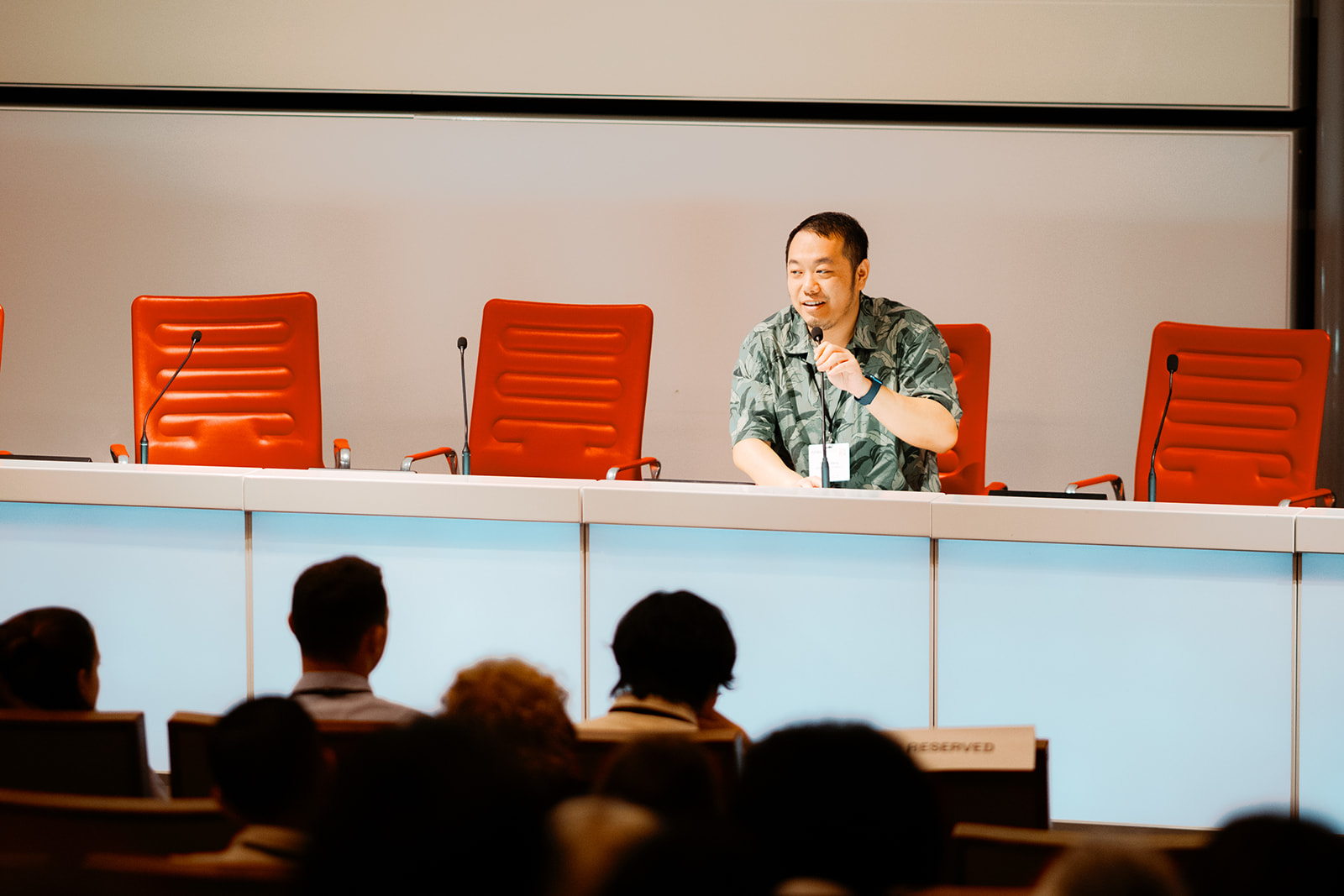
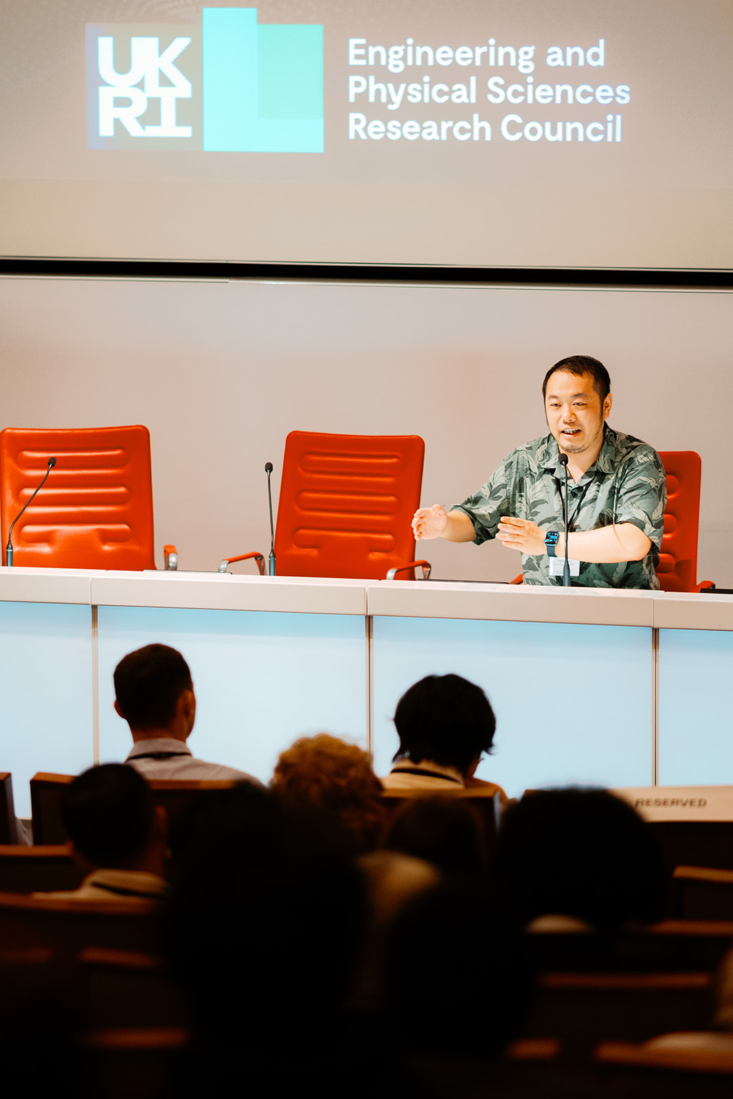
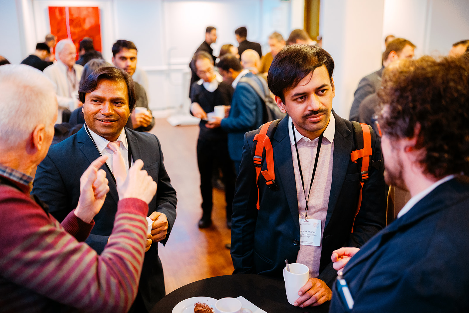
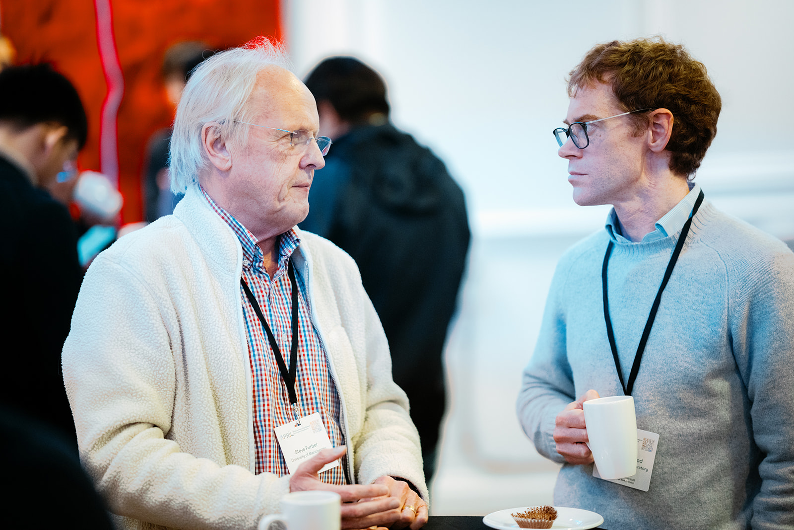
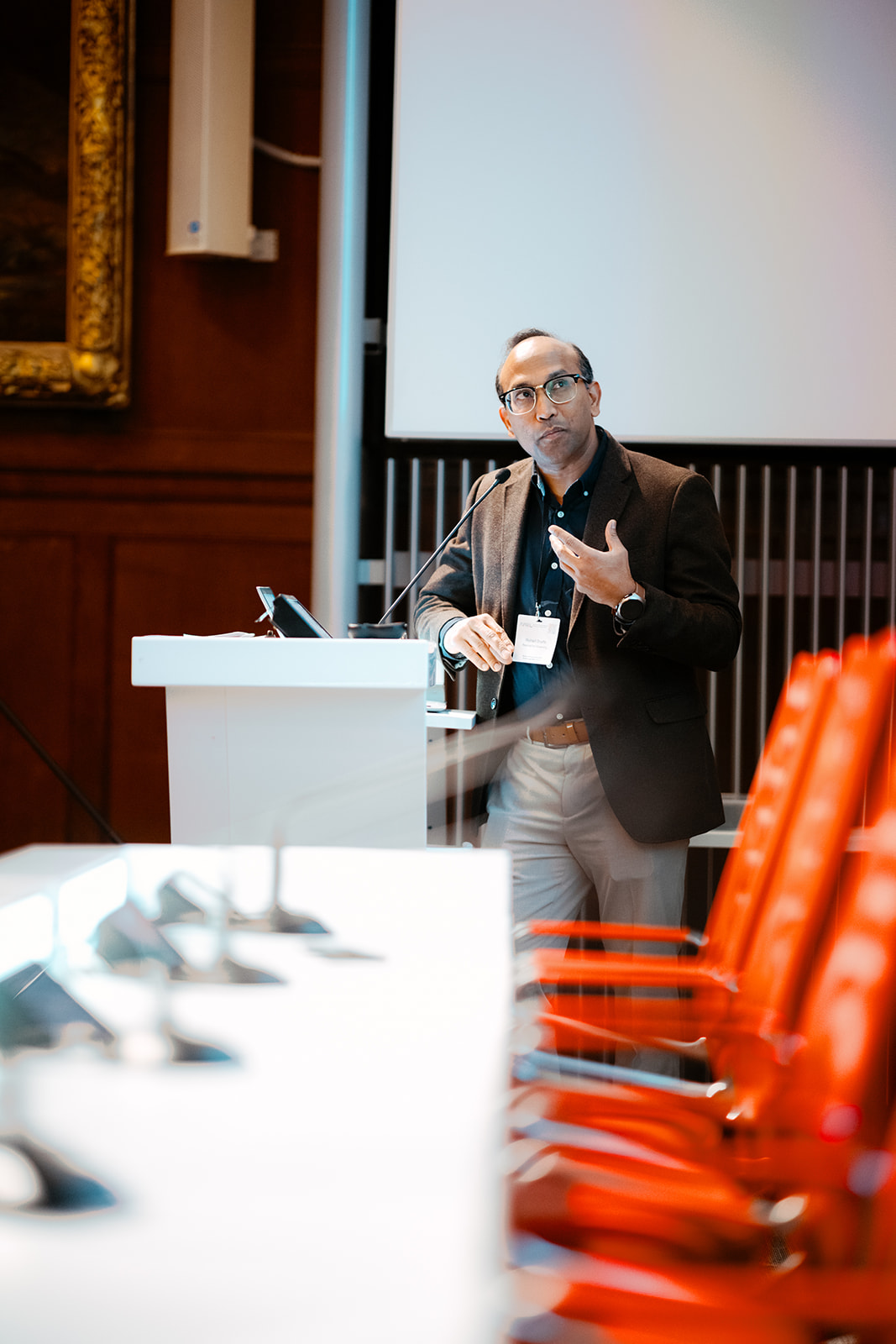
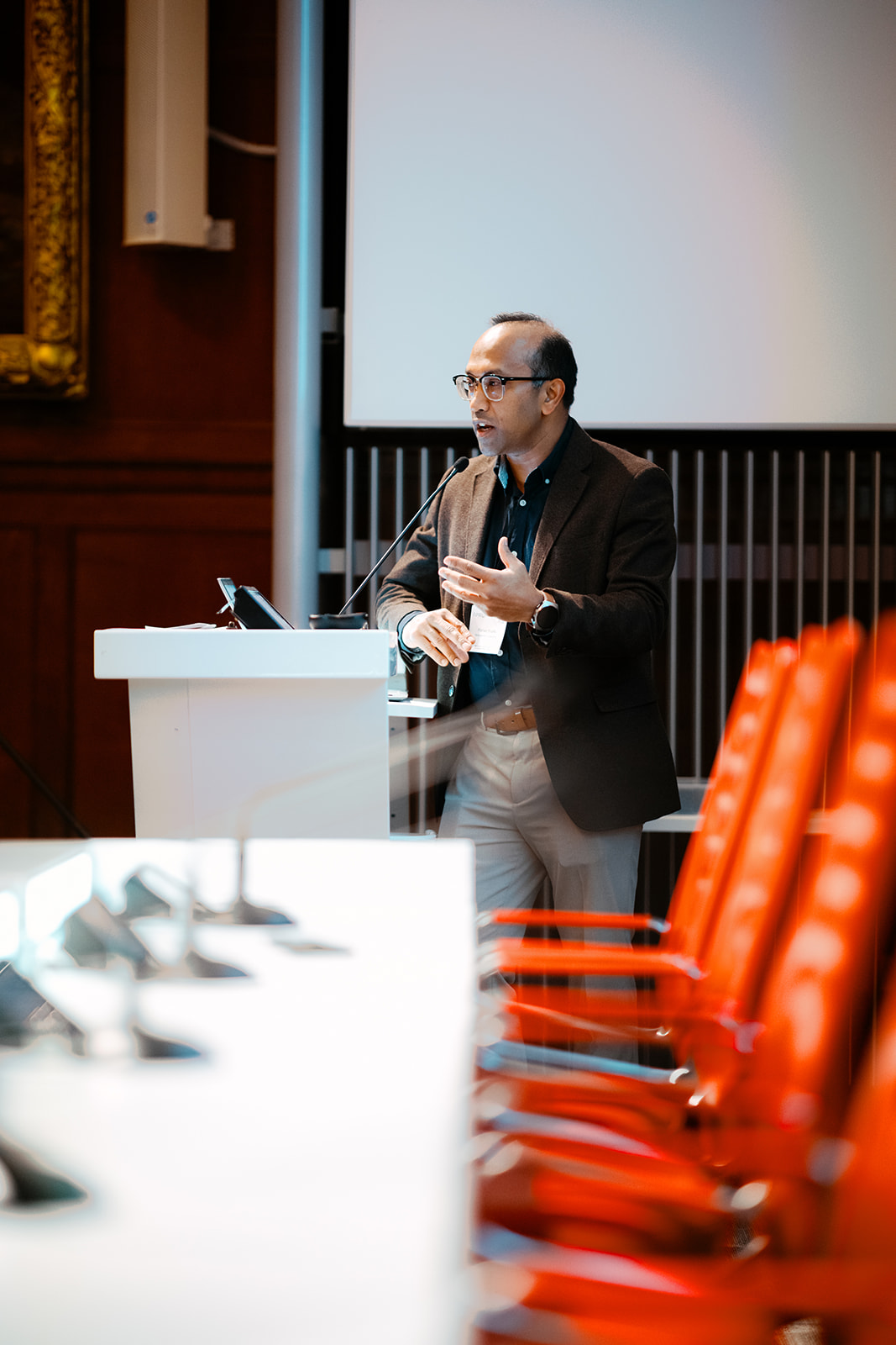
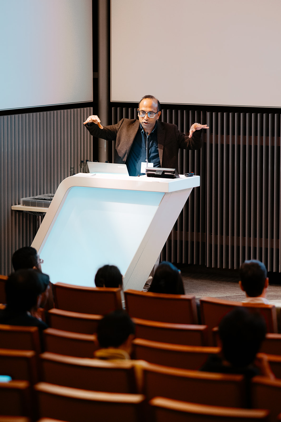
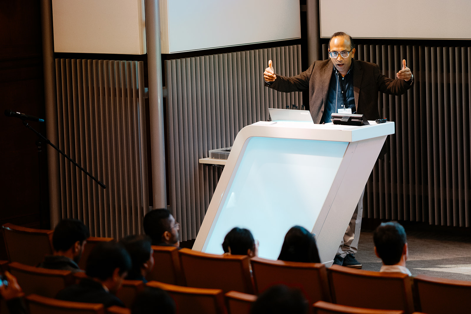
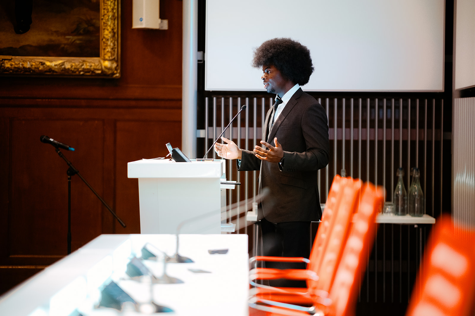
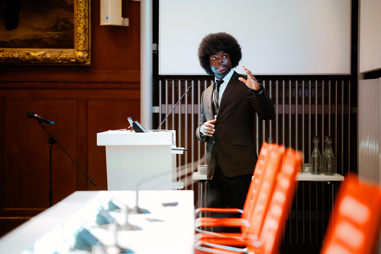
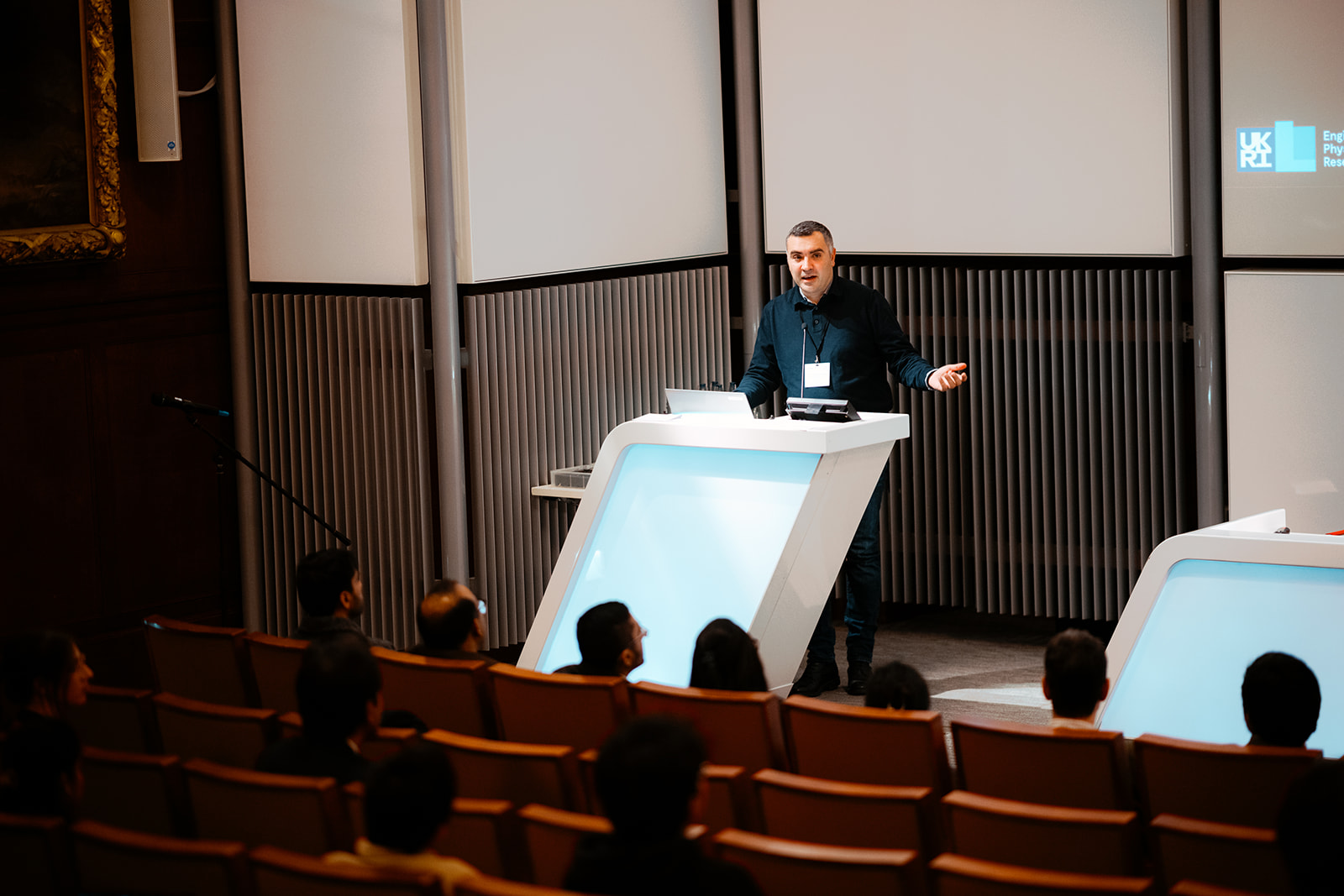
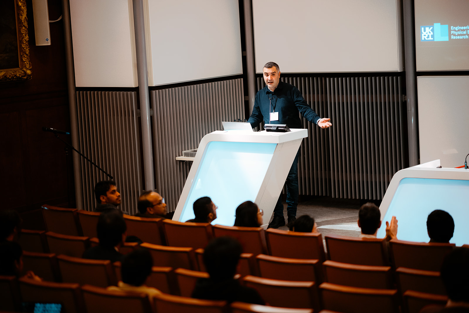
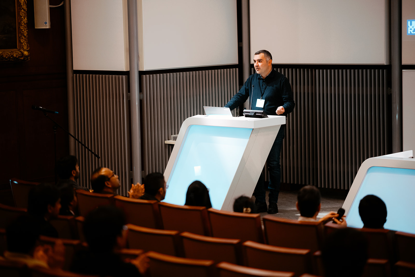
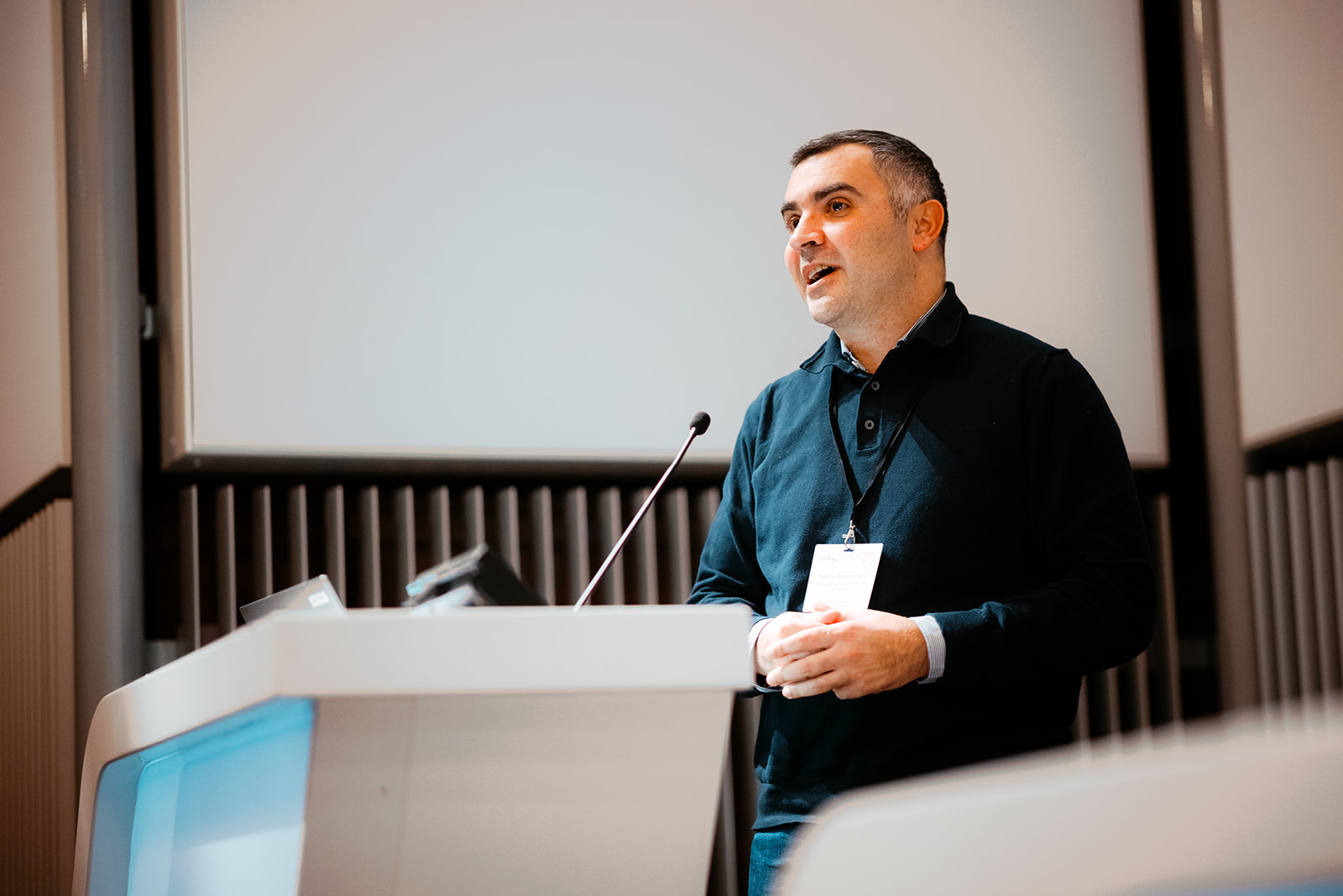
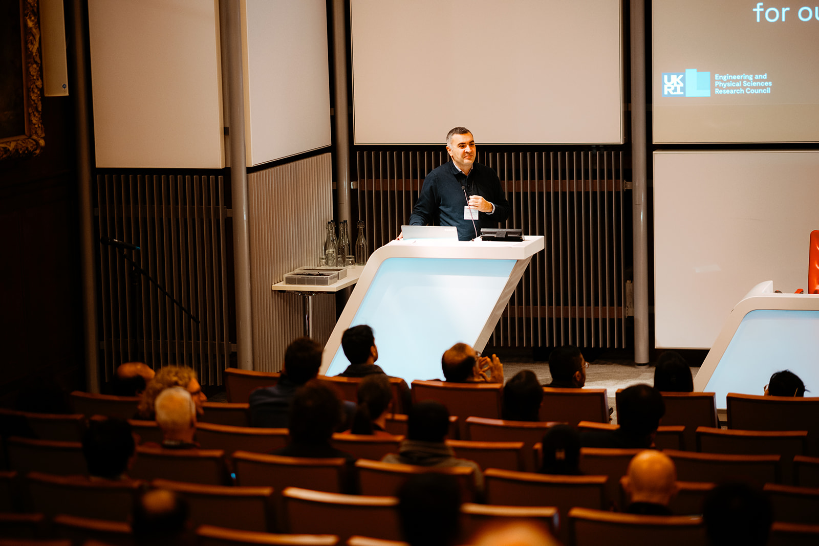
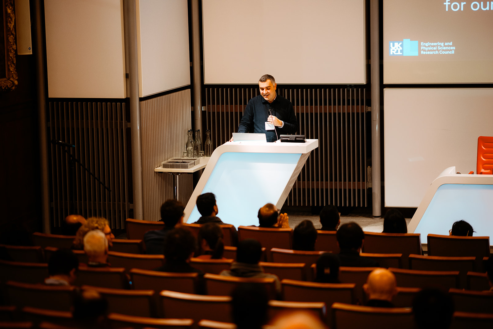
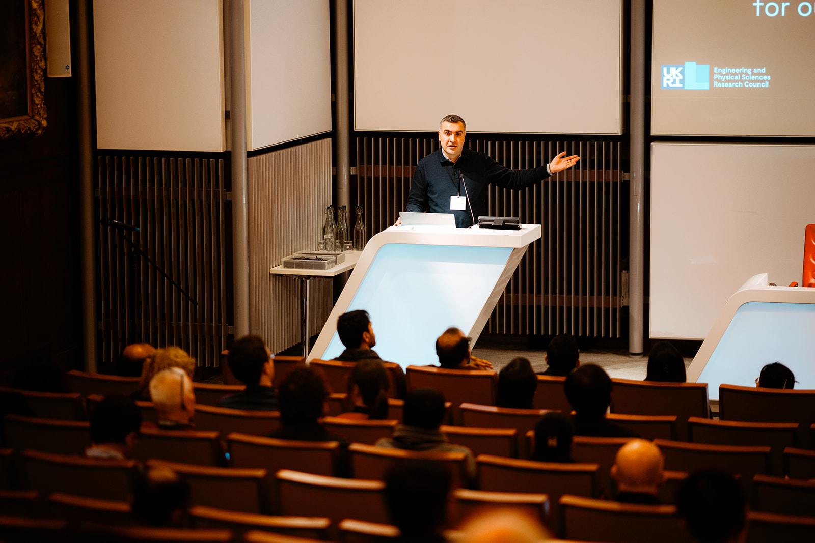
The APRIL AI Hub's Second Annual Summit will showcase progress from our Researchers, Seed Funding Grant Holders, and Google DeepMind Research Ready Interns 2025. We look forward to updating industry partners, stakeholders, and anyone else interested in our research on the amazing work our Hub has been doing over the past year.
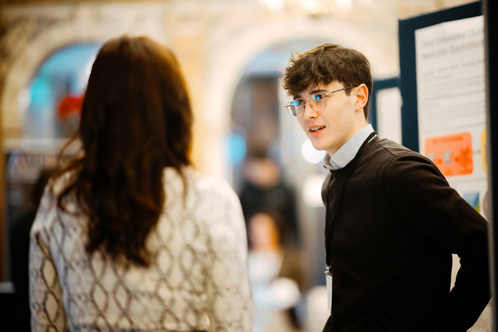
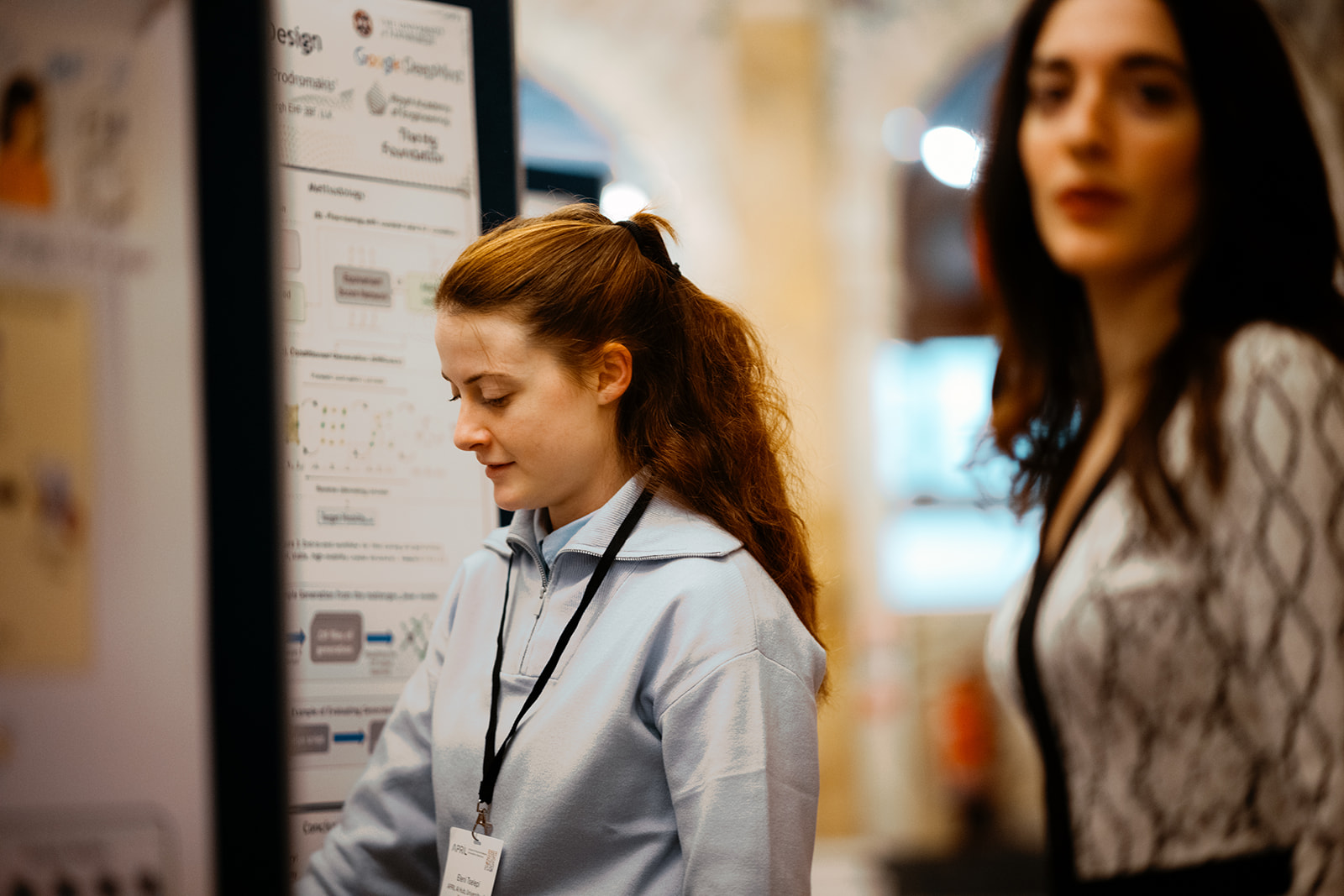
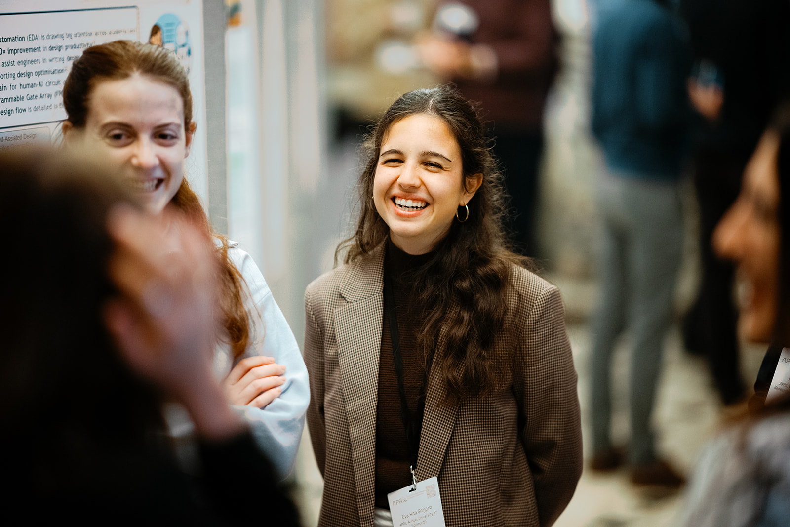
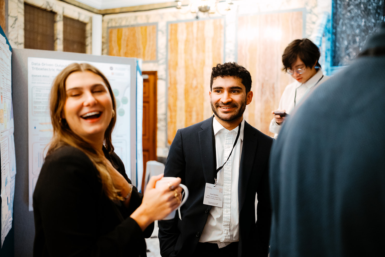
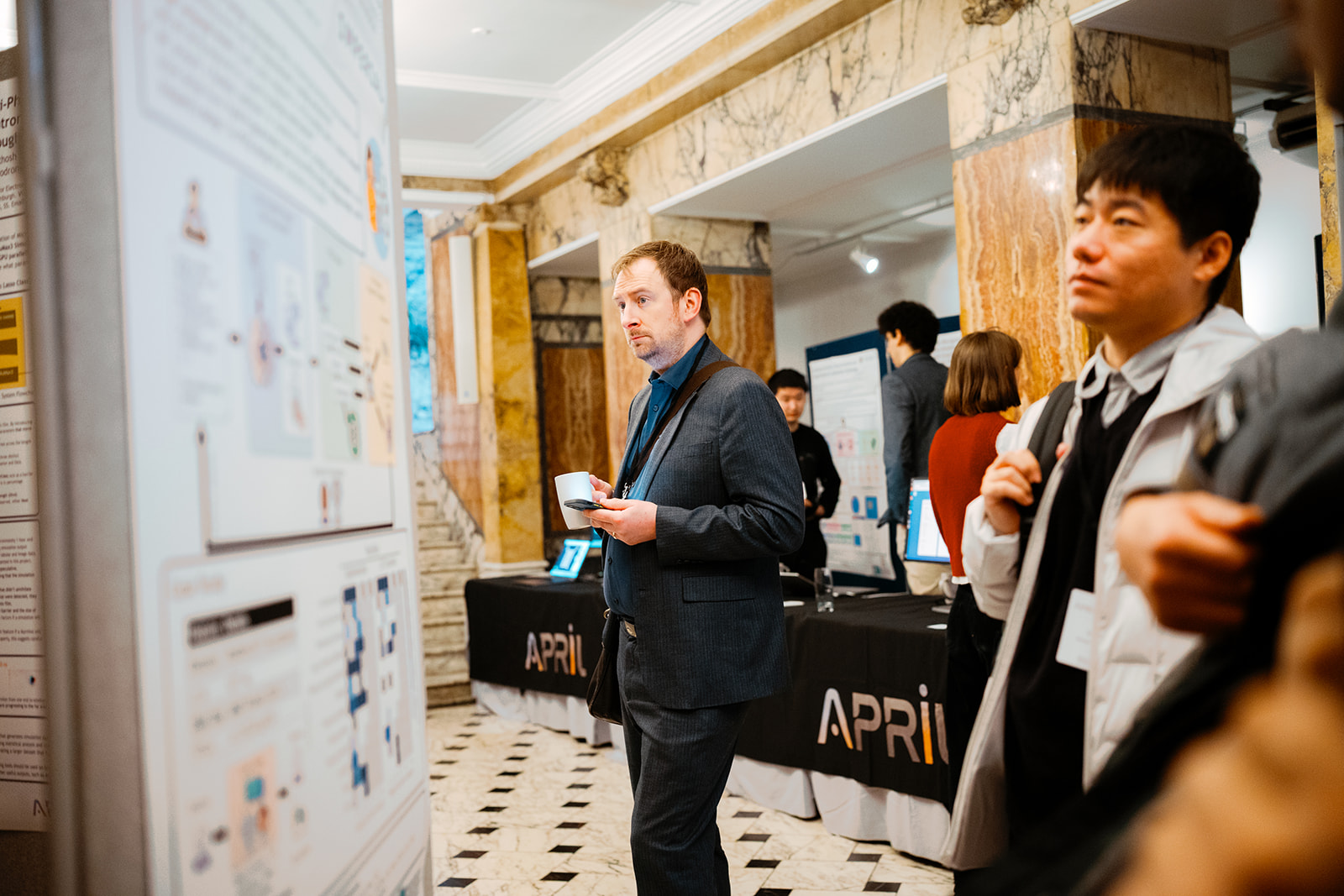
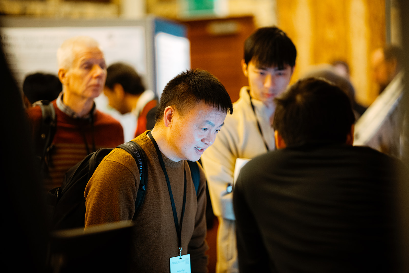
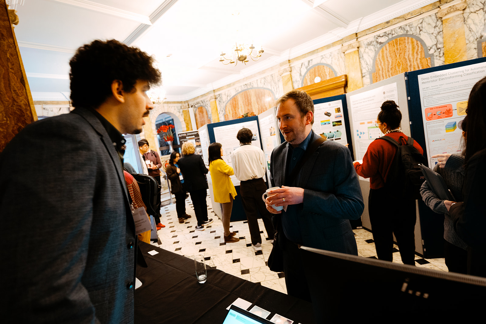
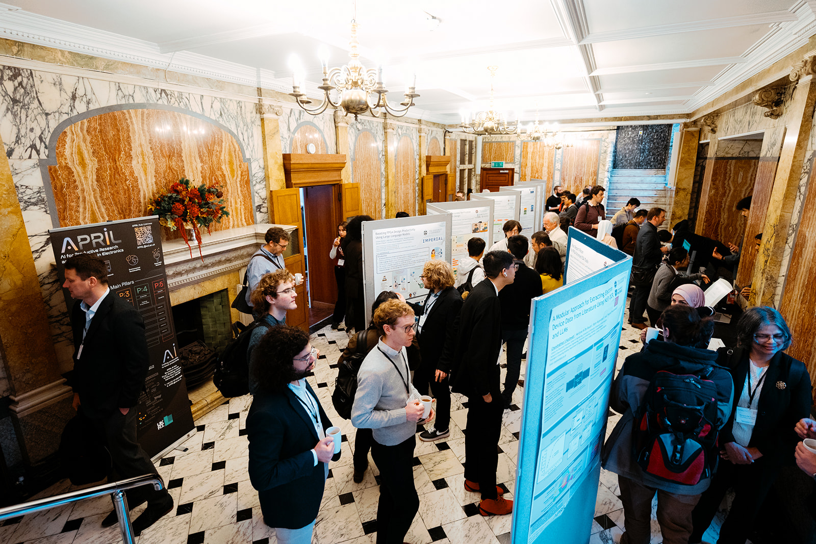
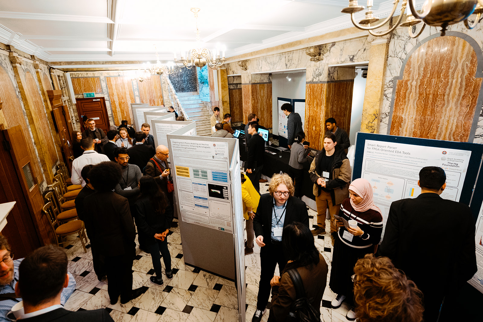
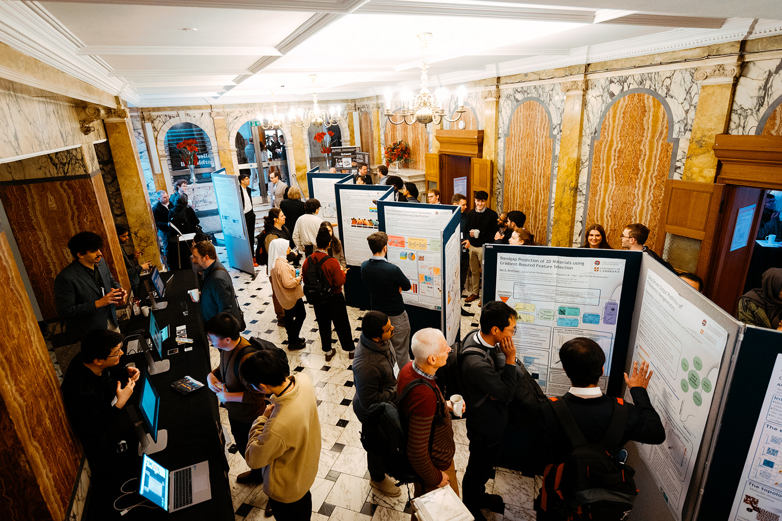
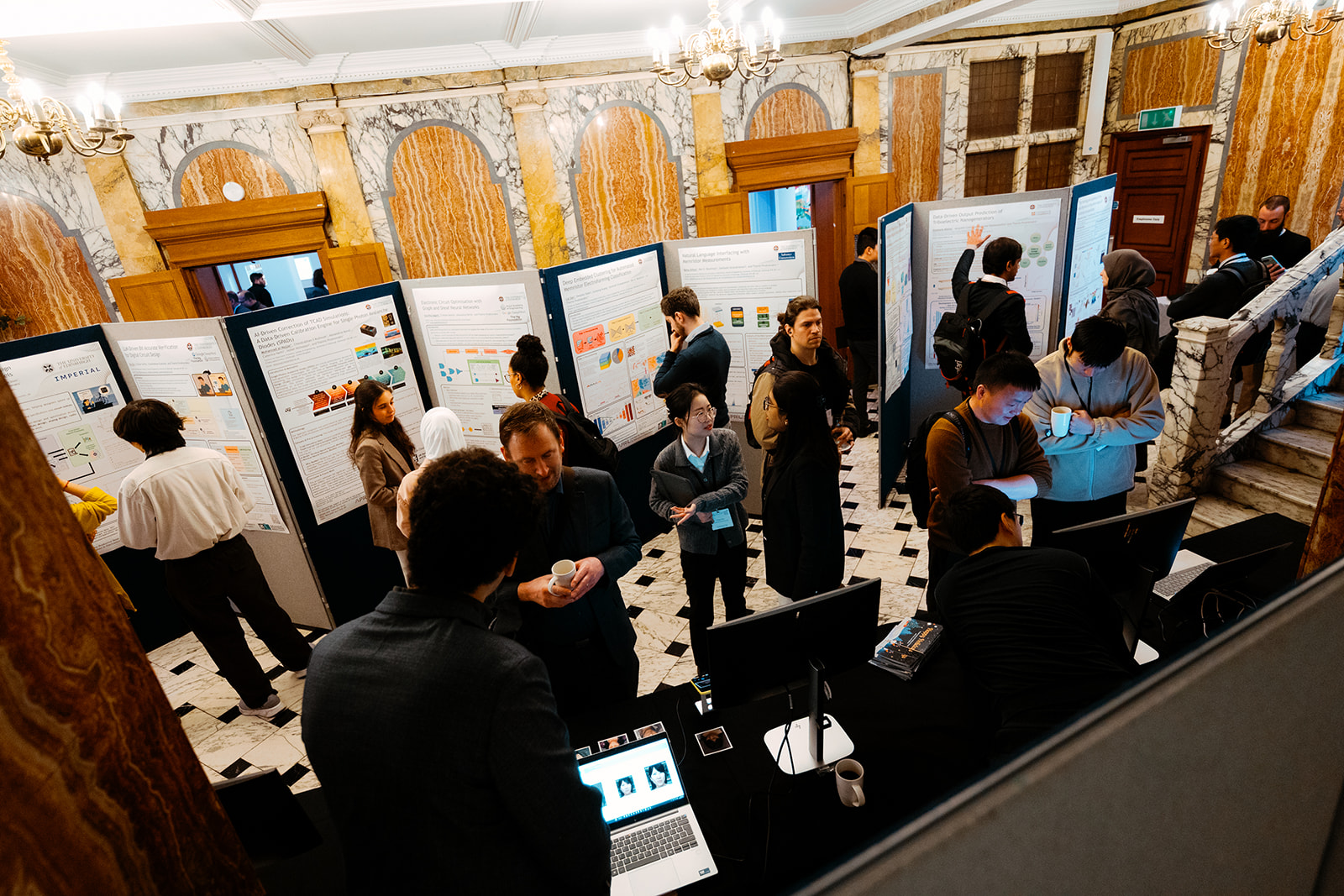
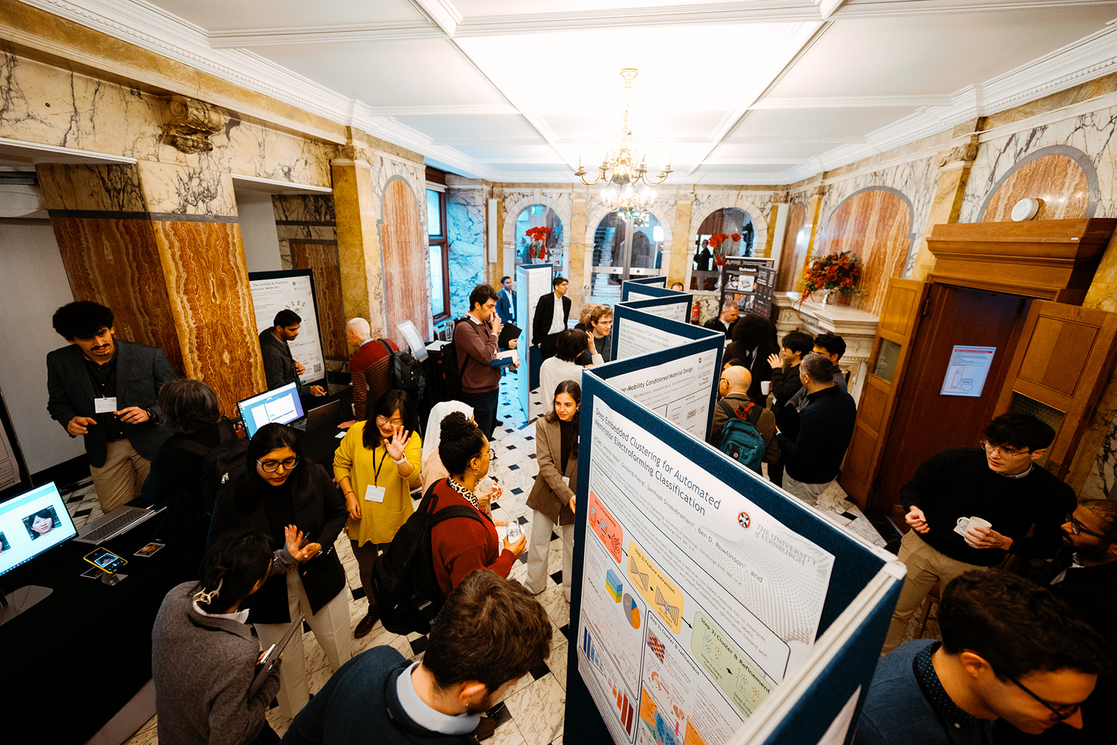
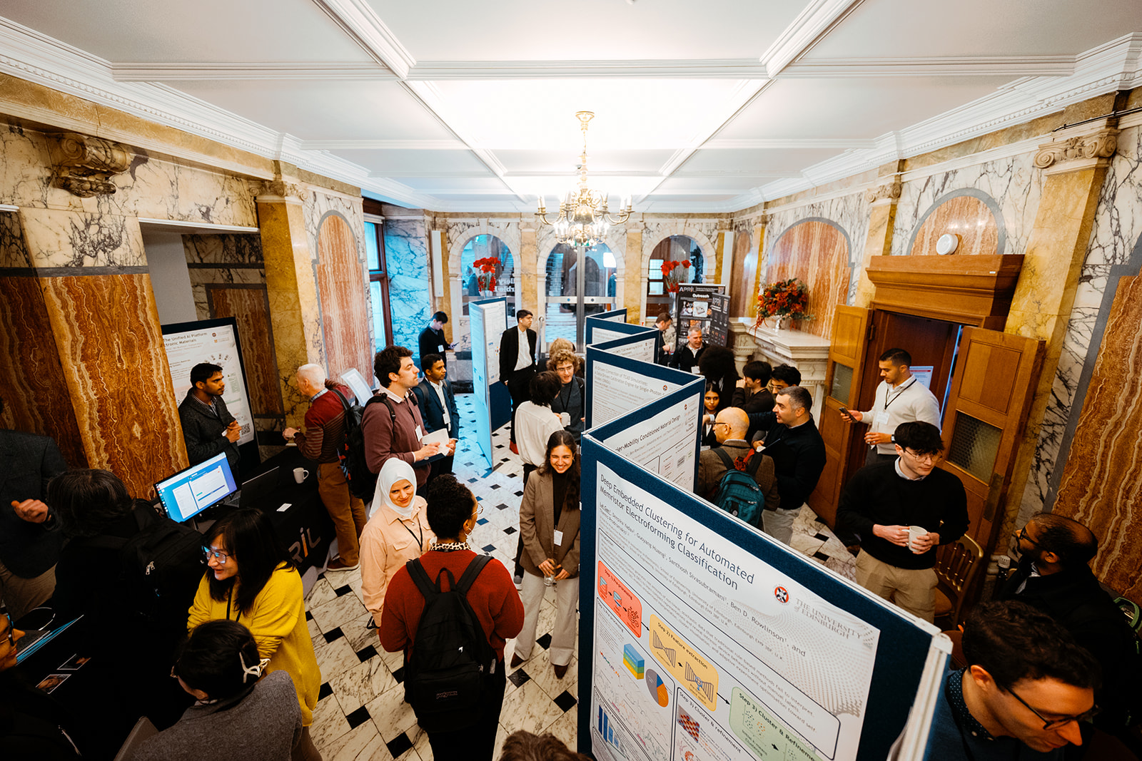
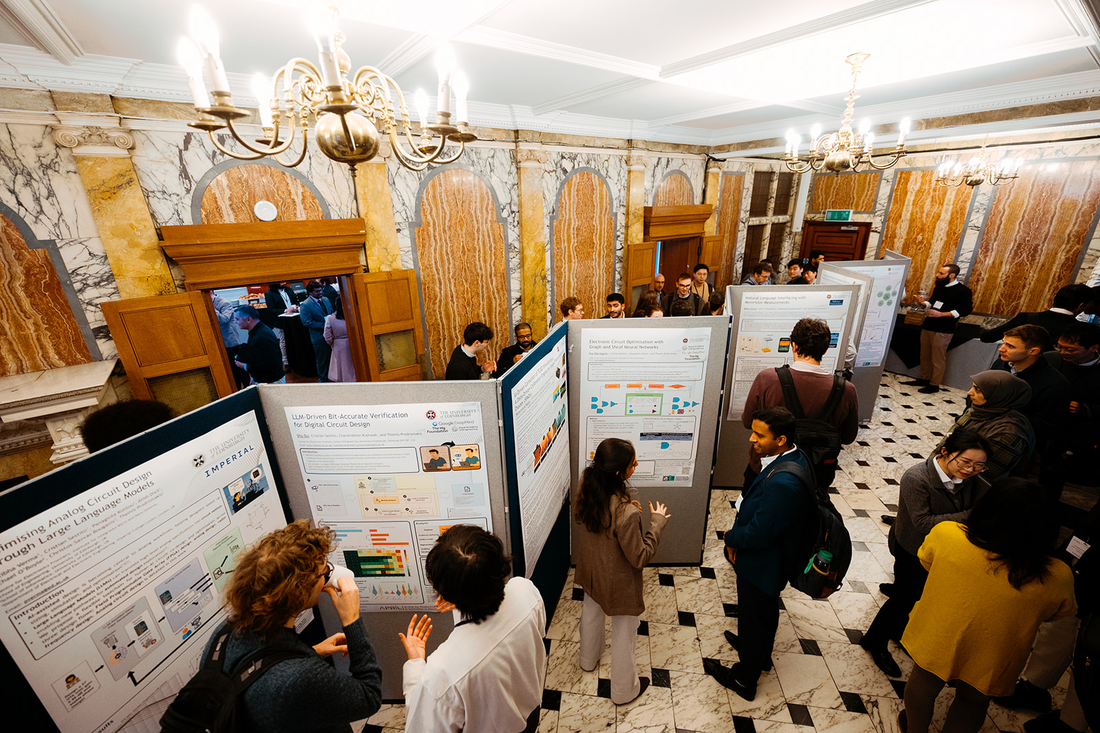
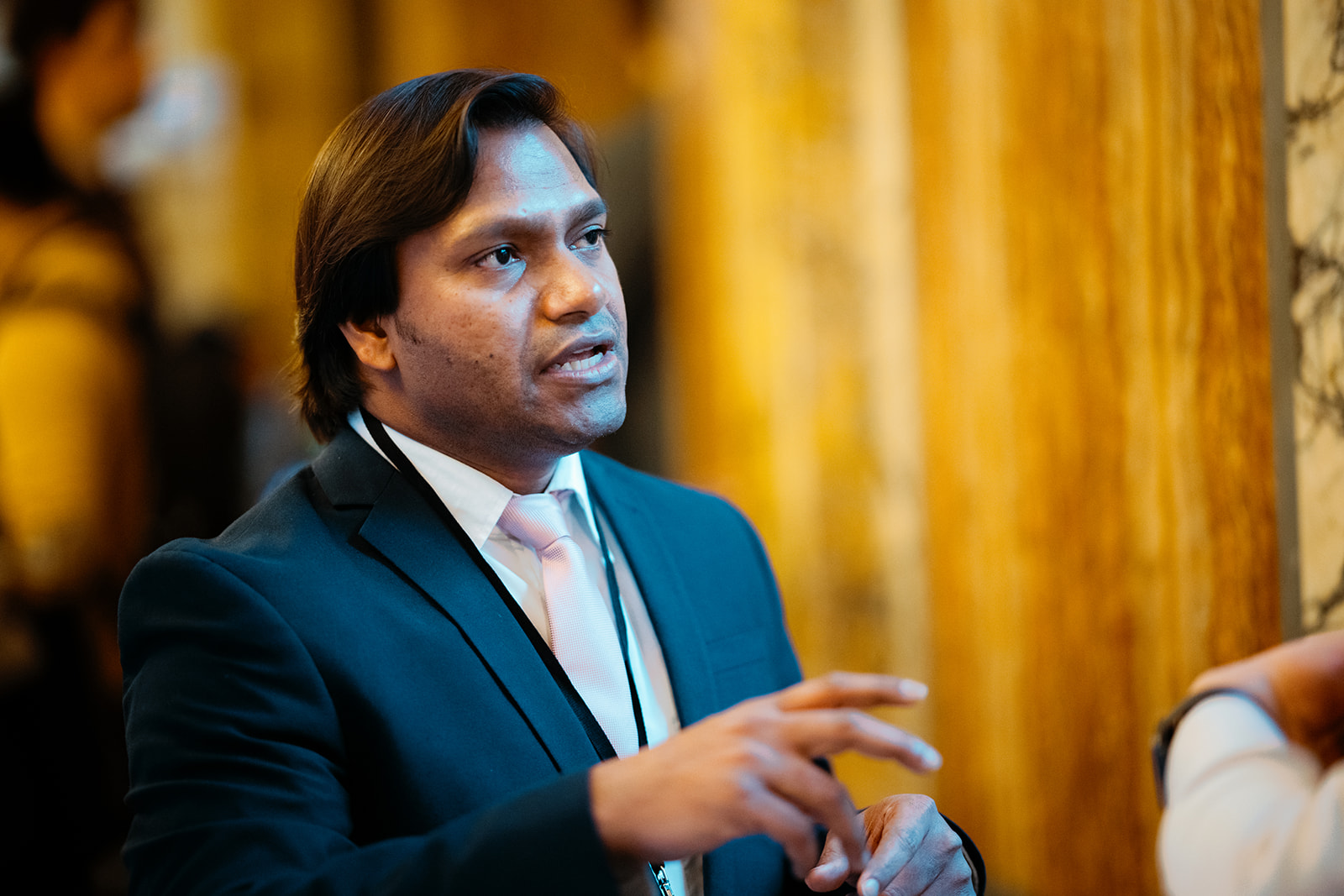
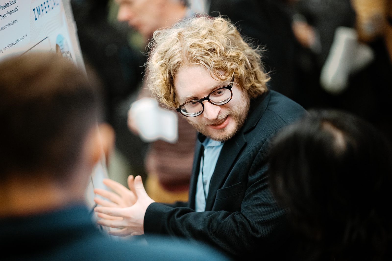
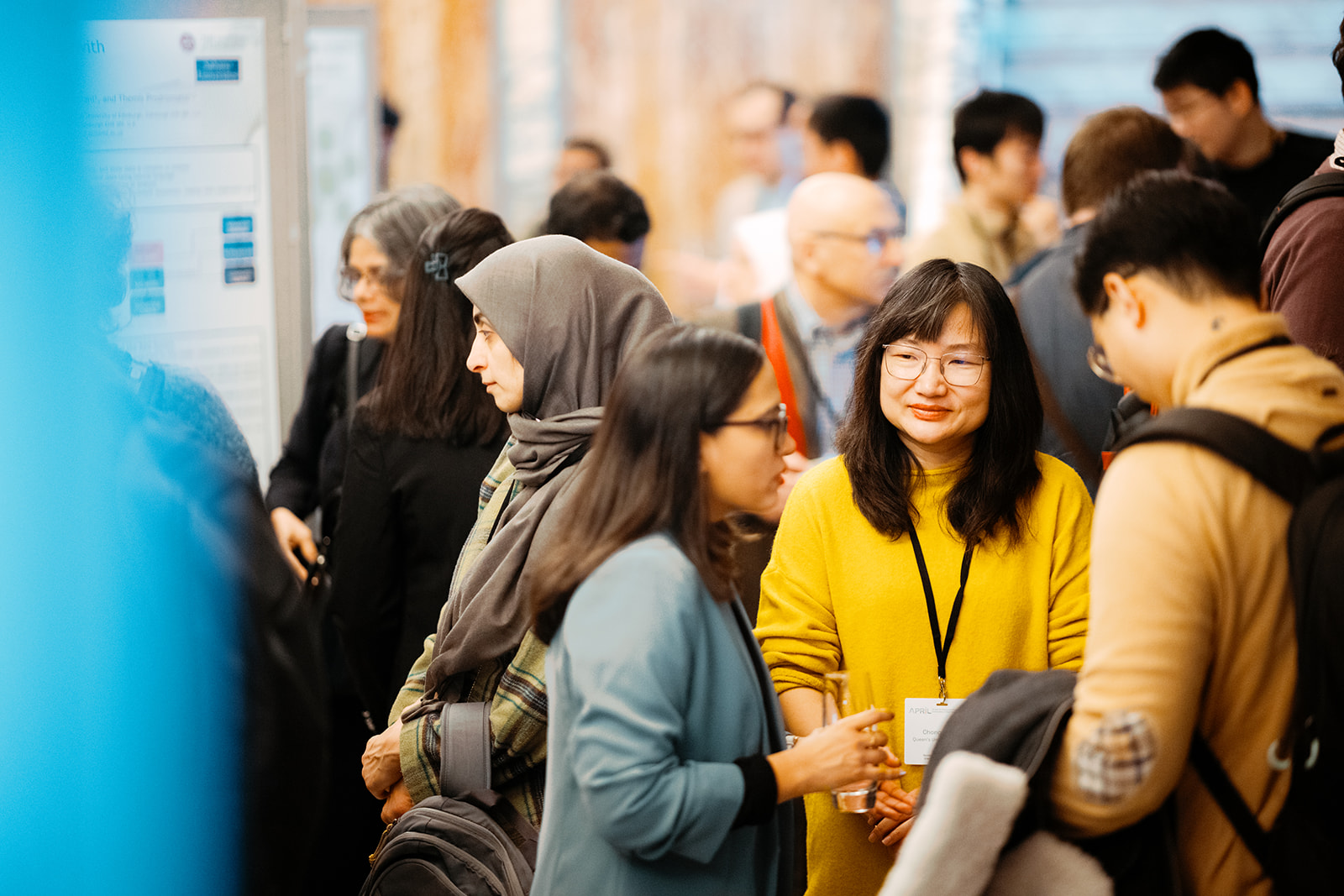
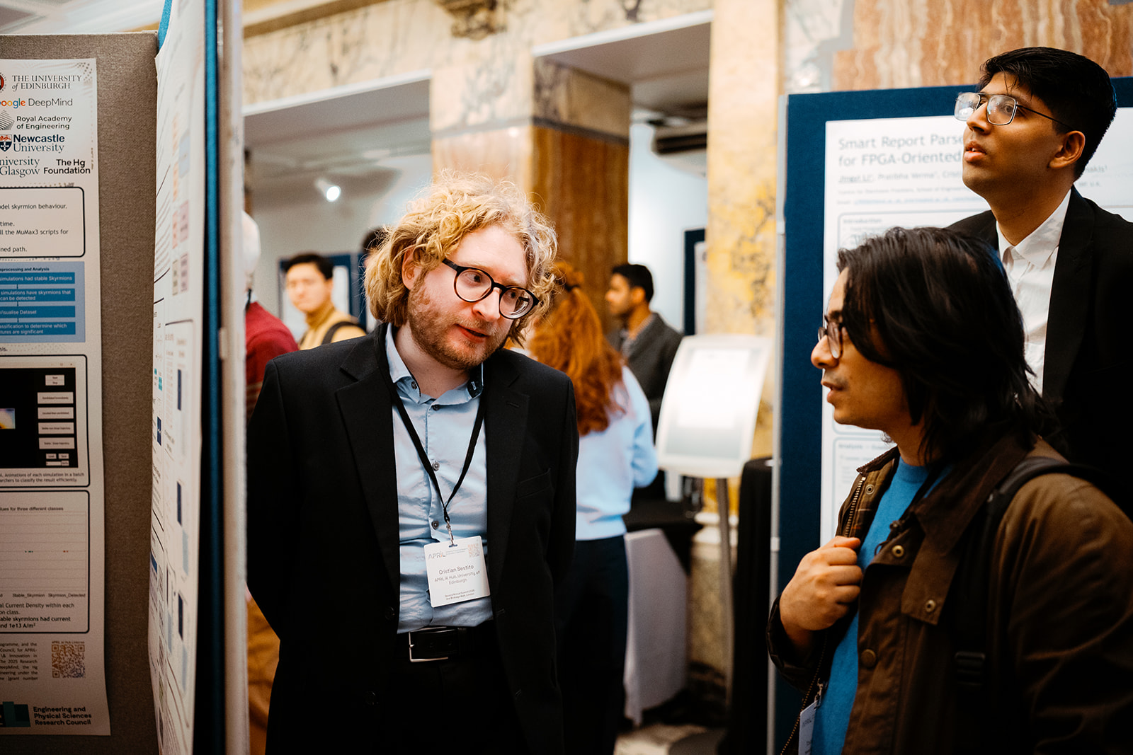
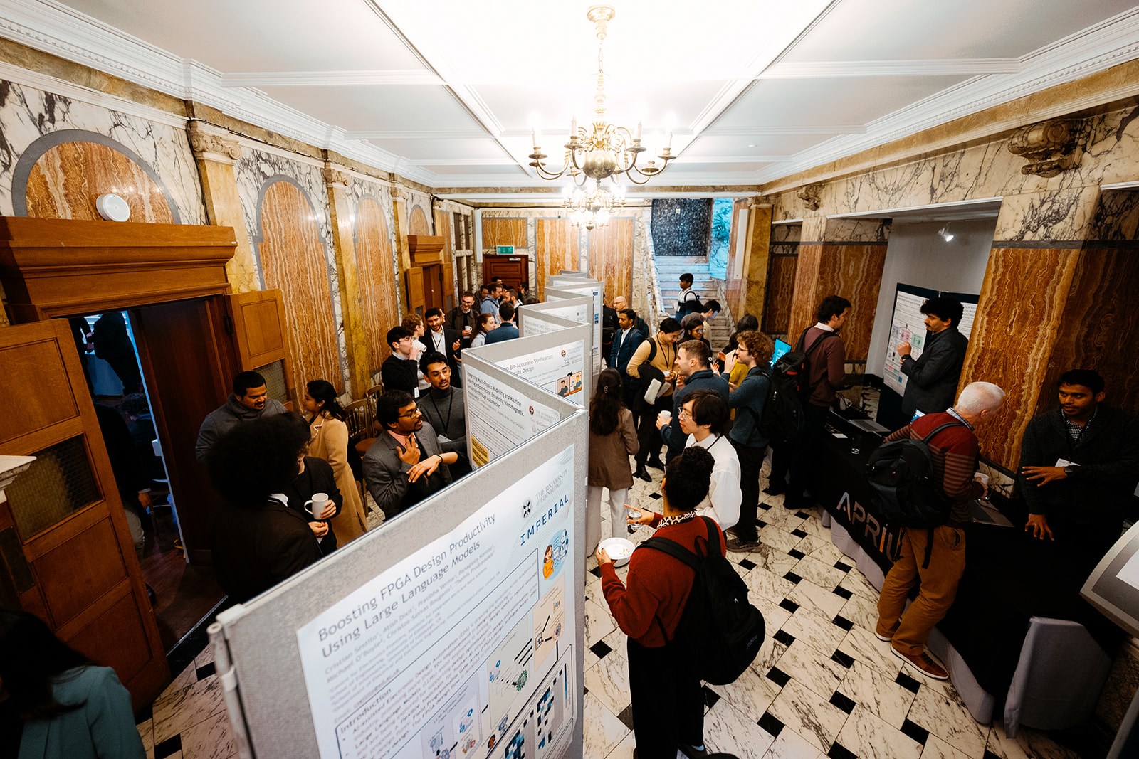
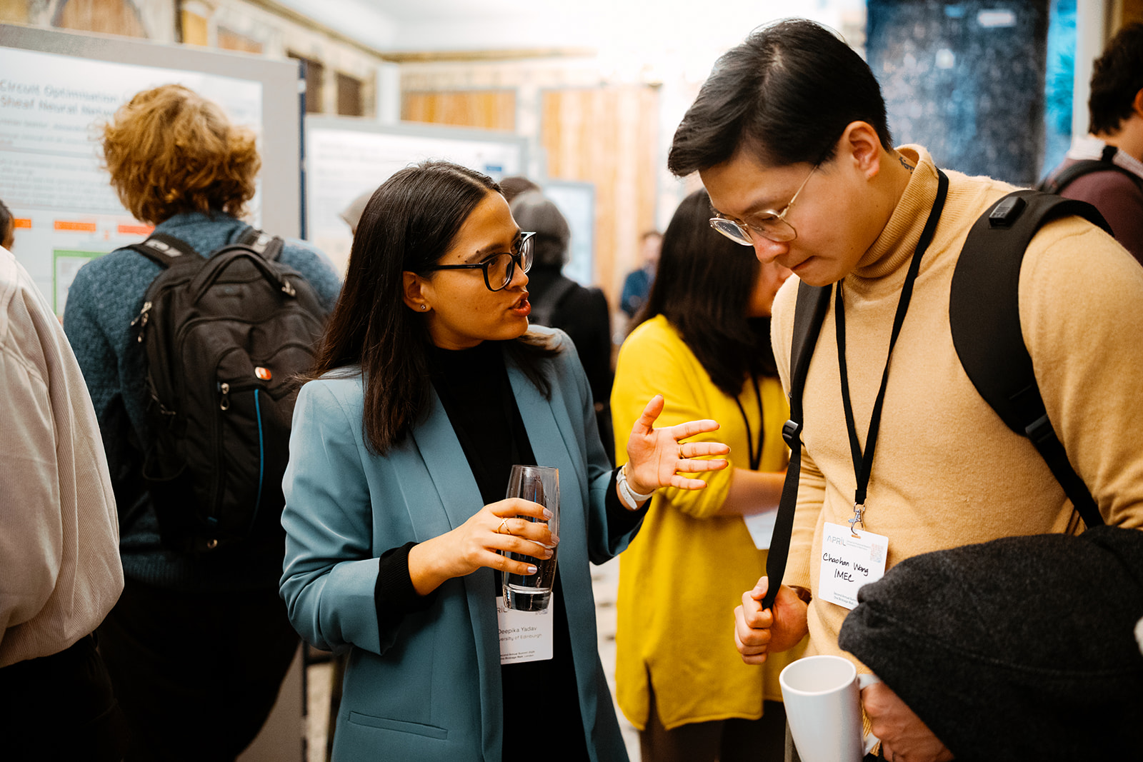
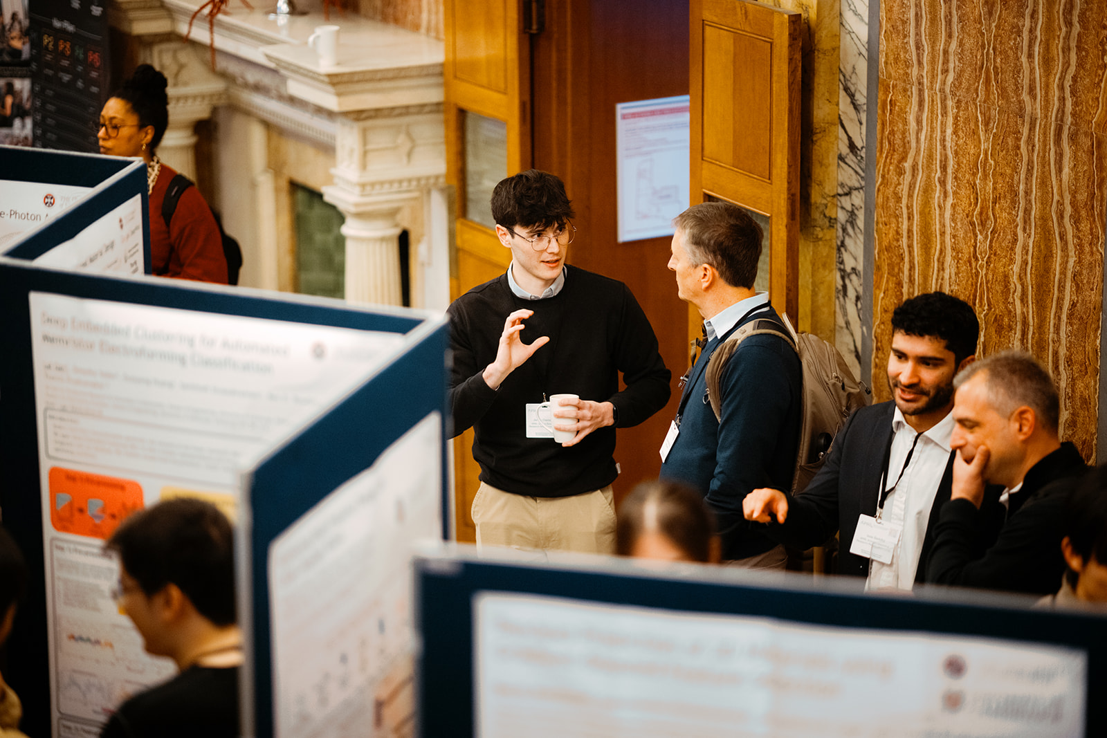
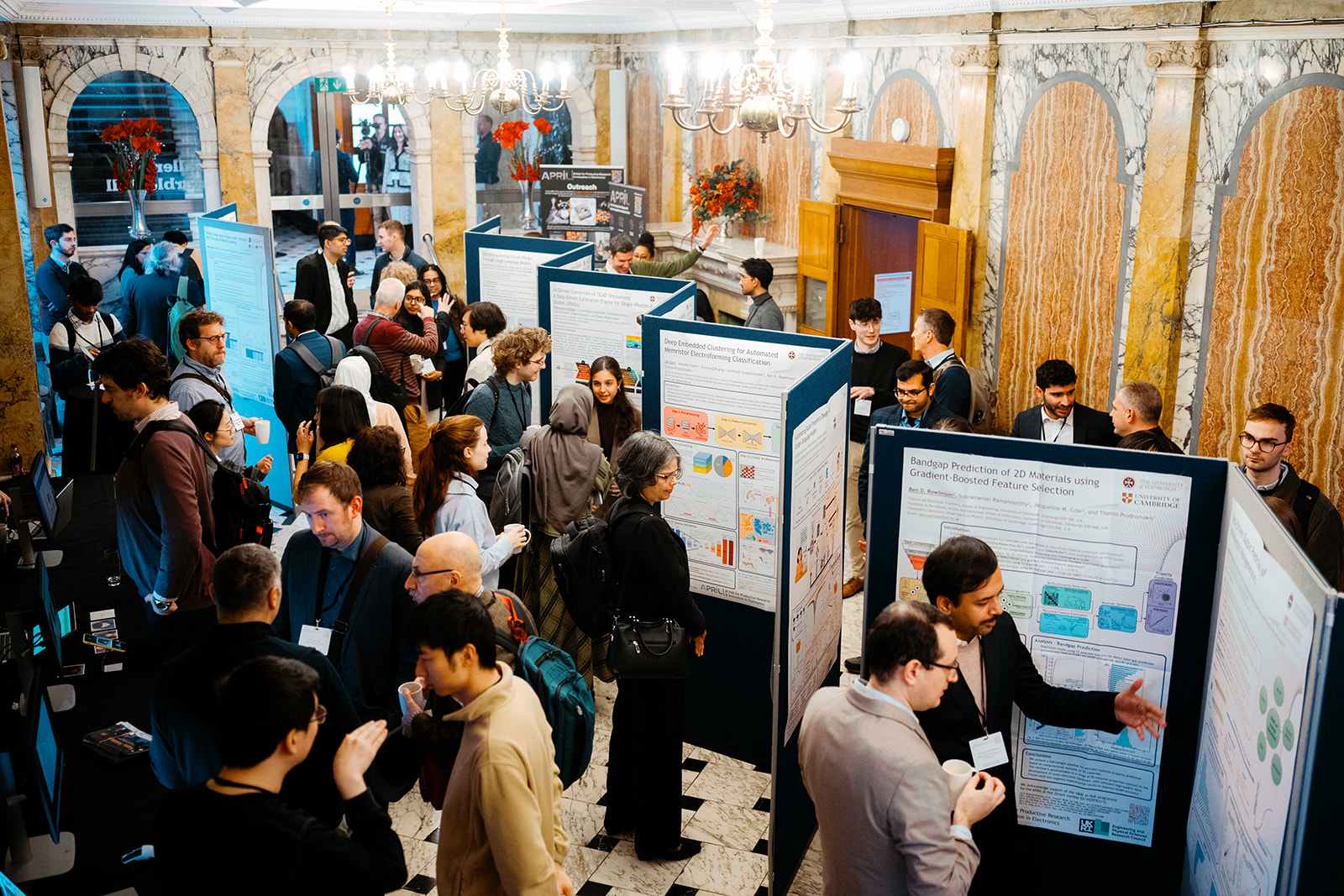
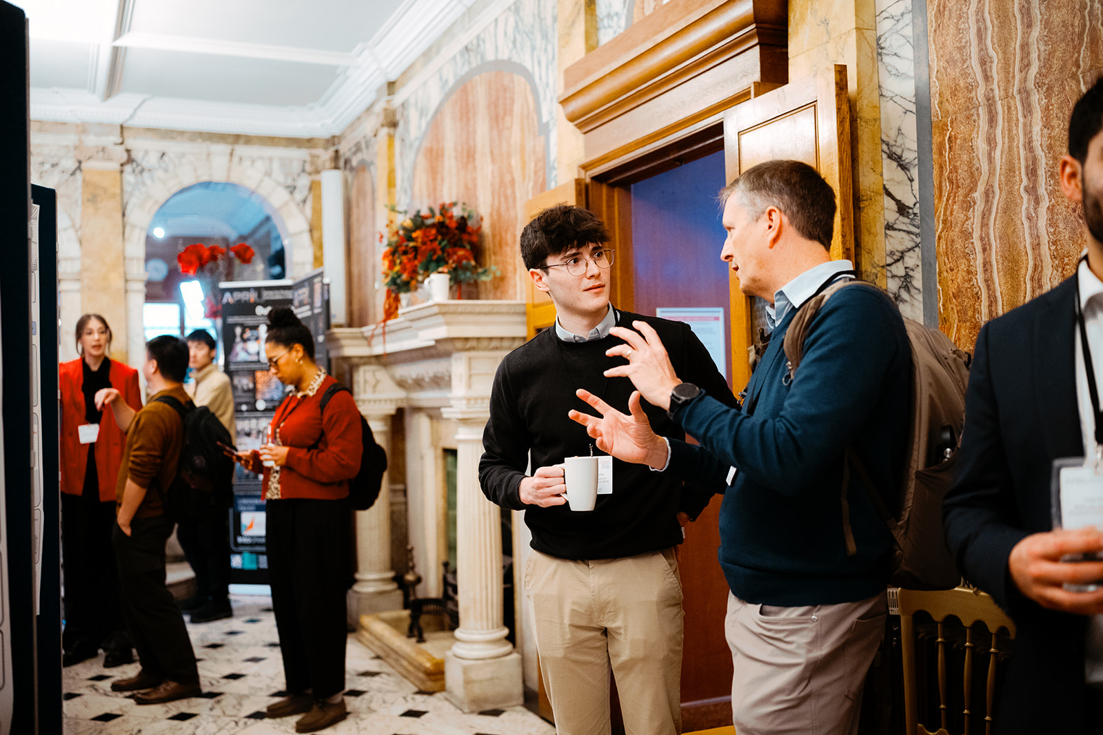
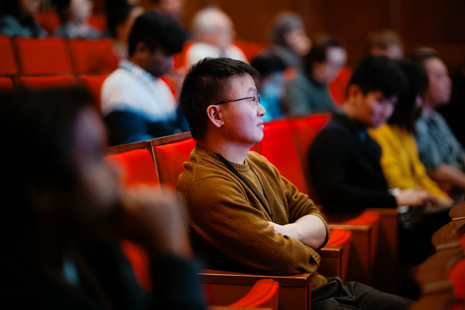
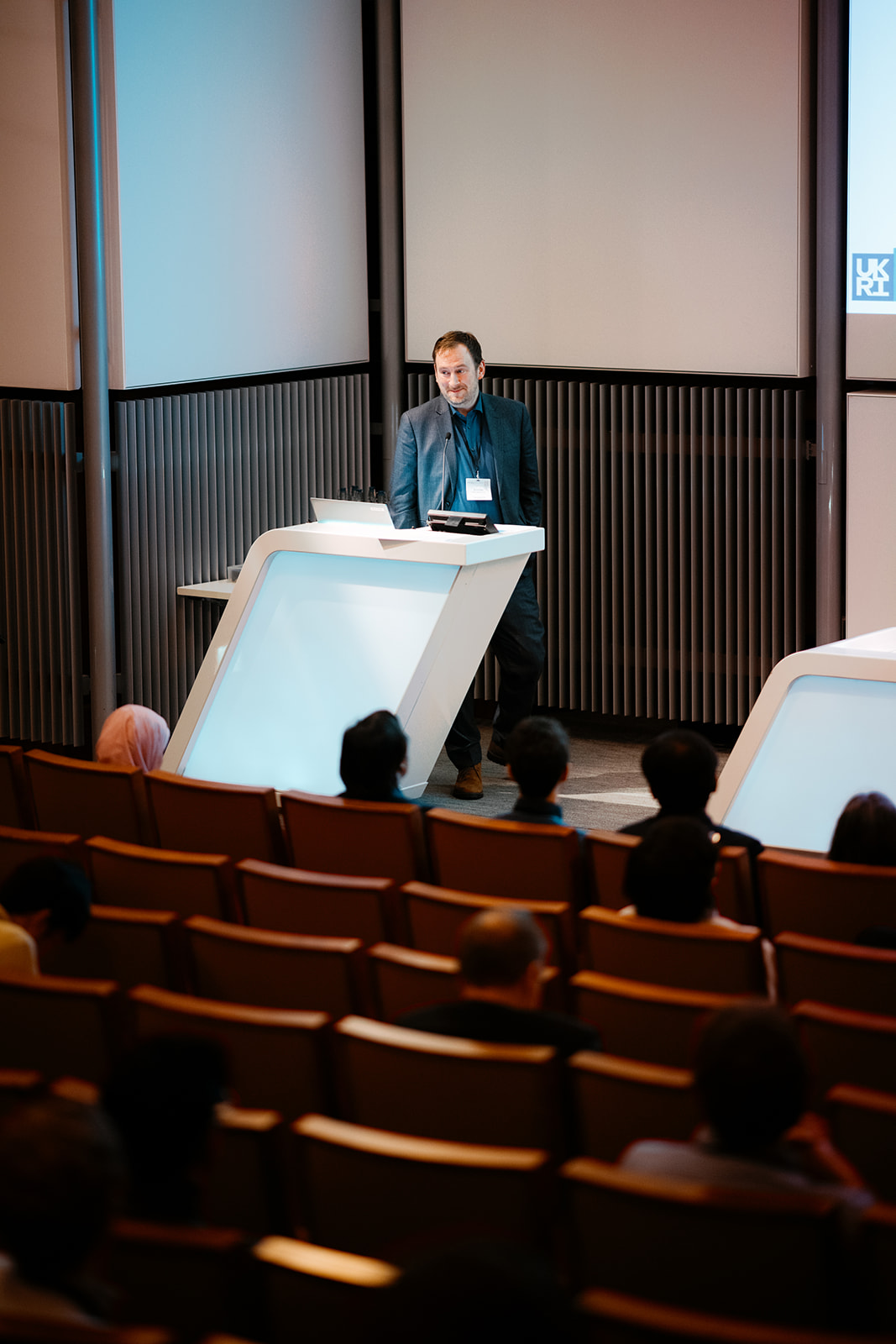
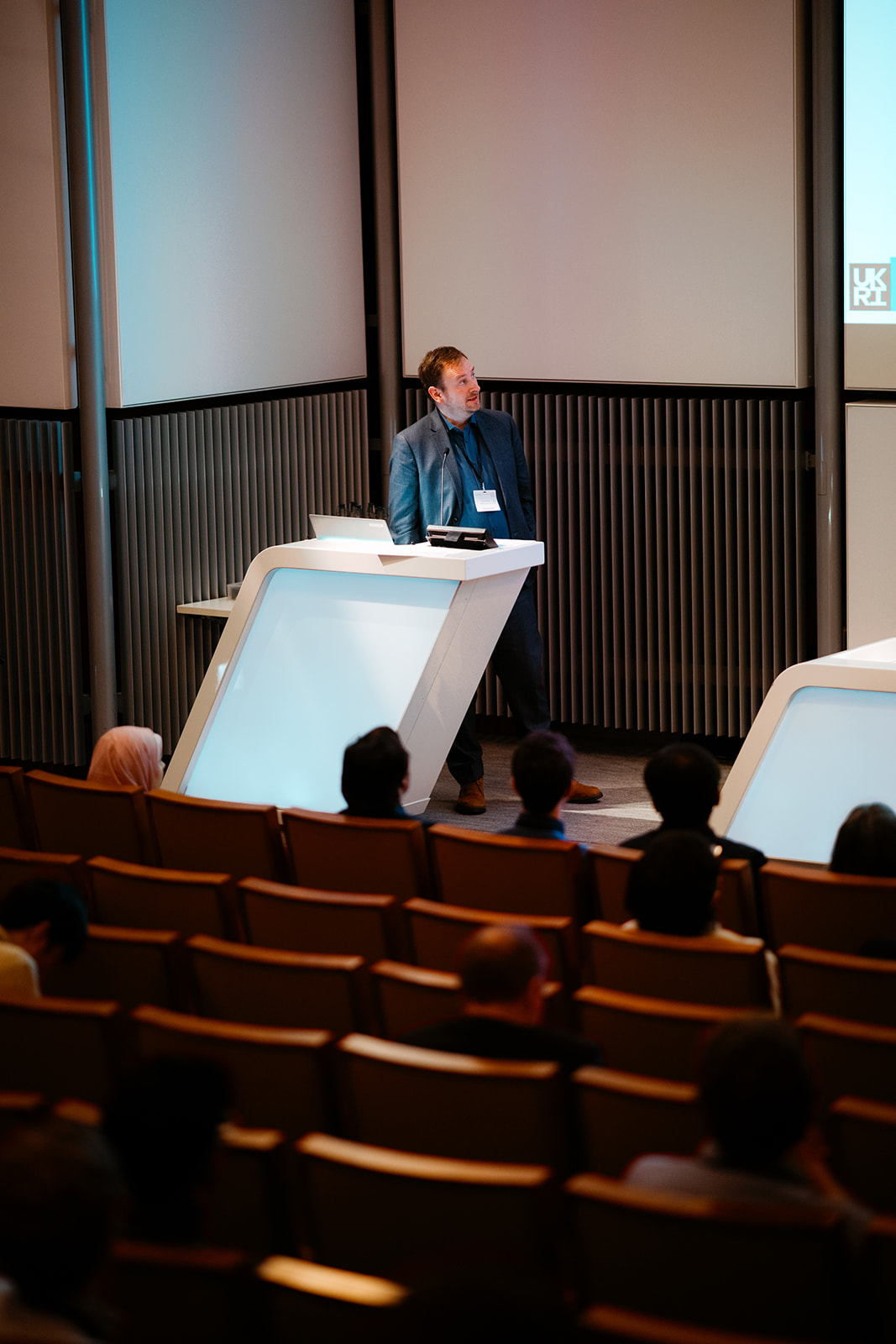
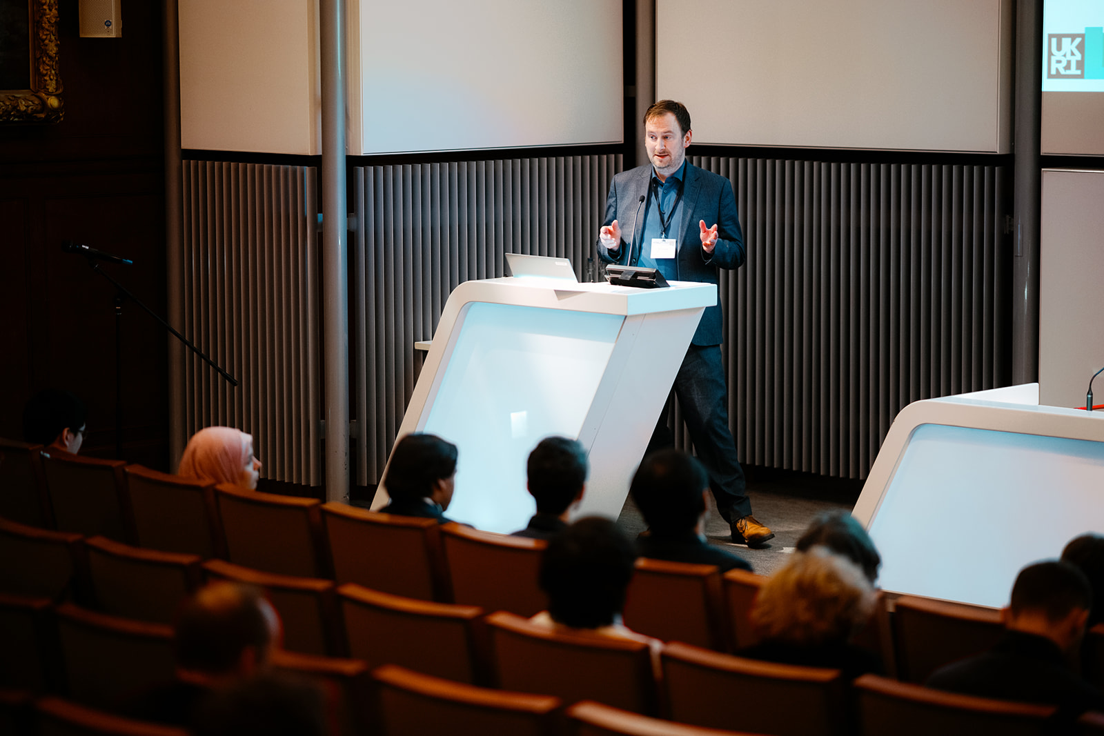
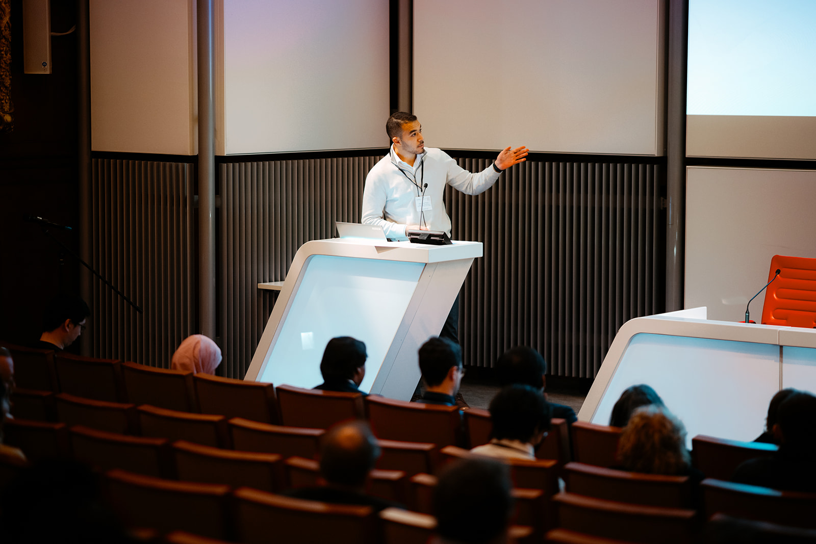
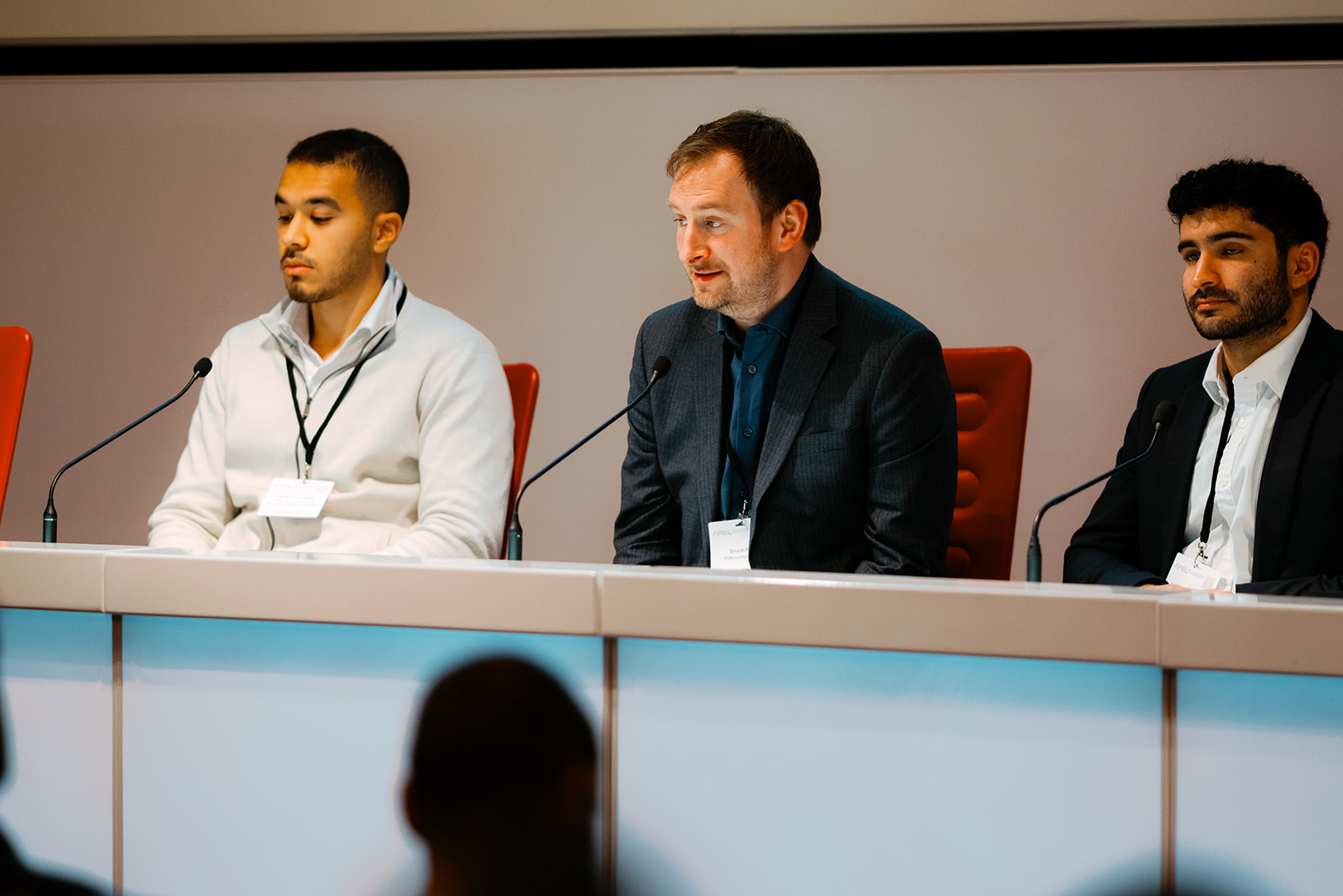
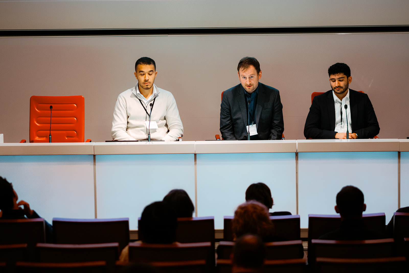
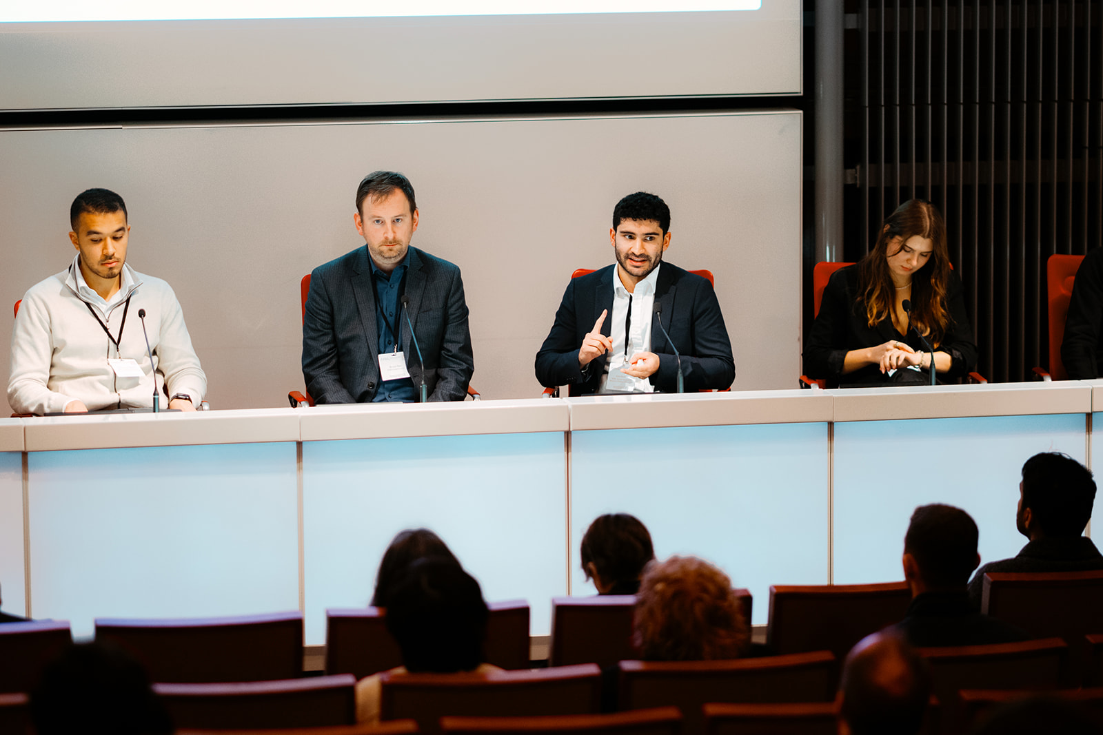
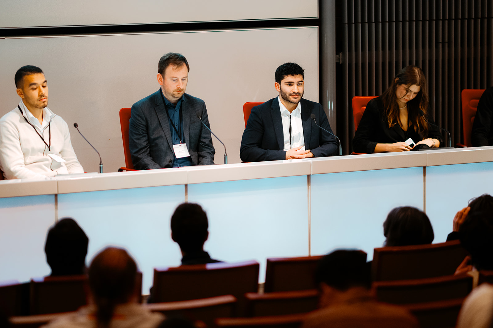
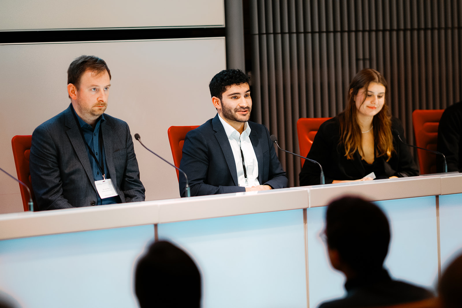
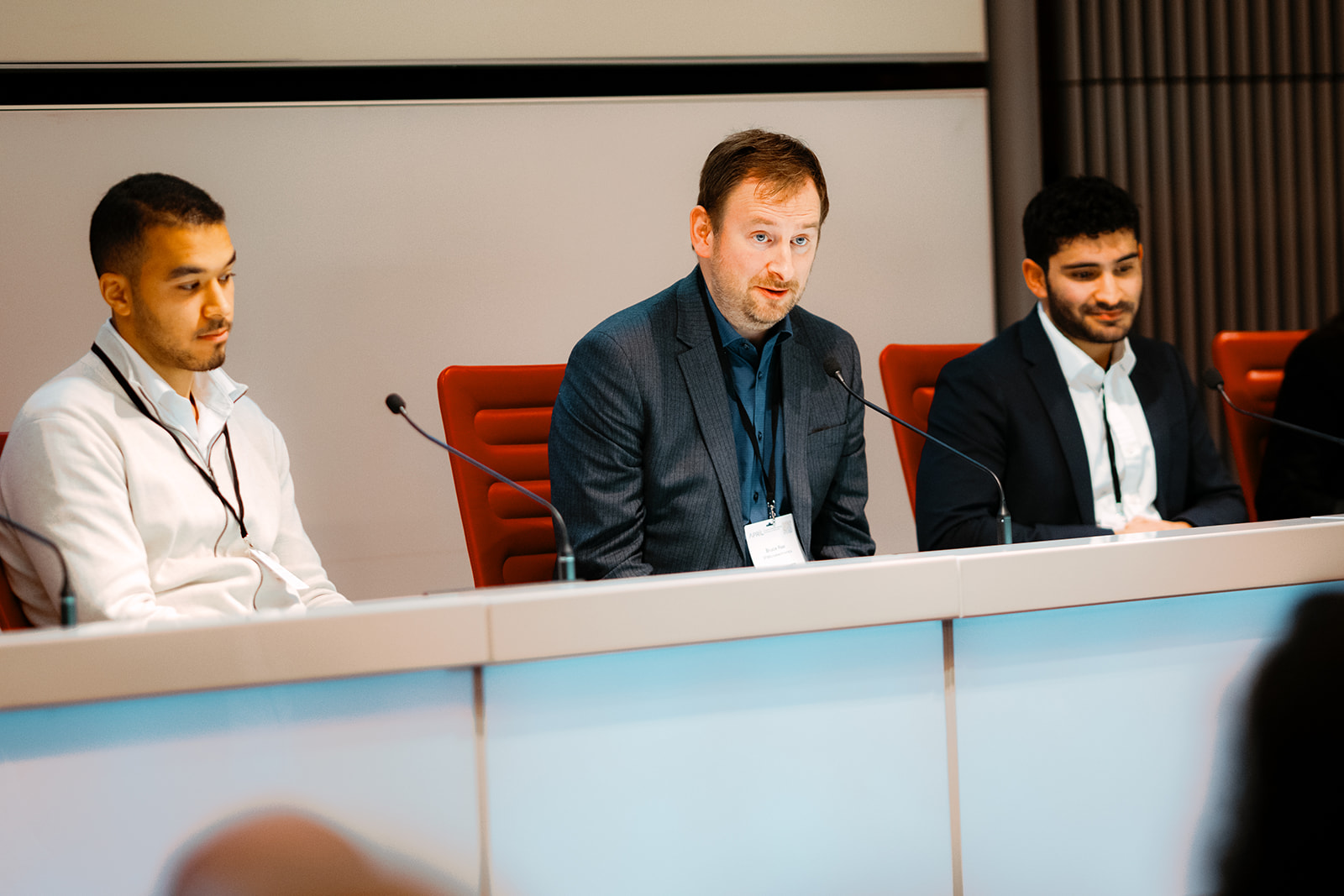
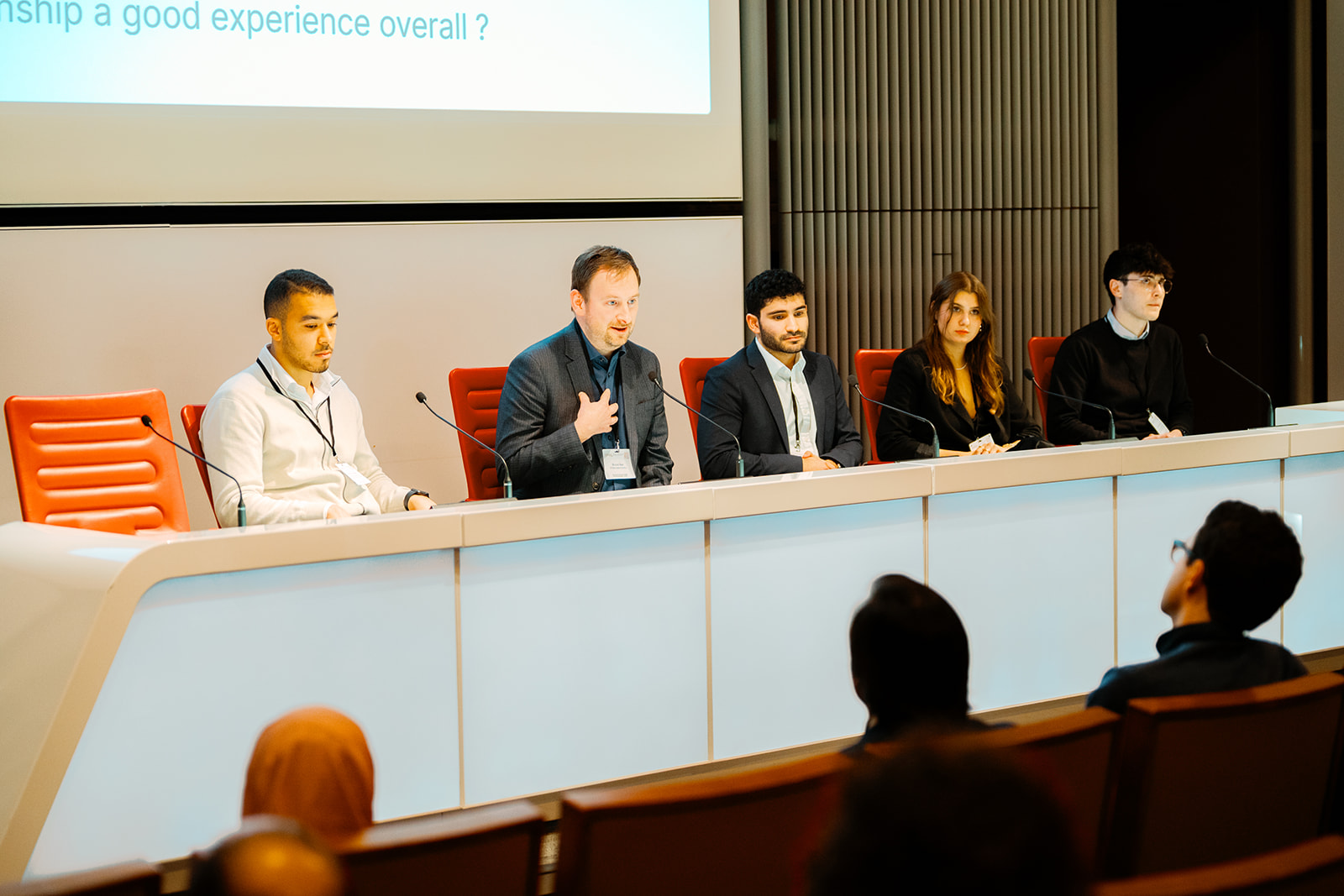
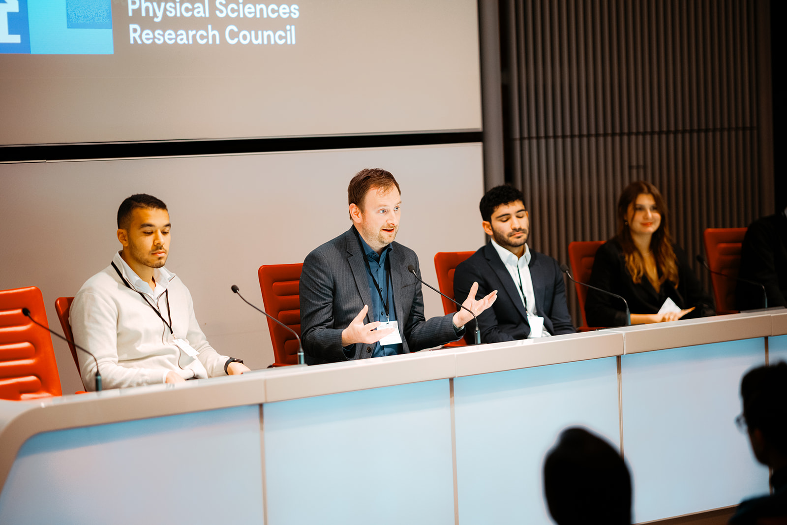
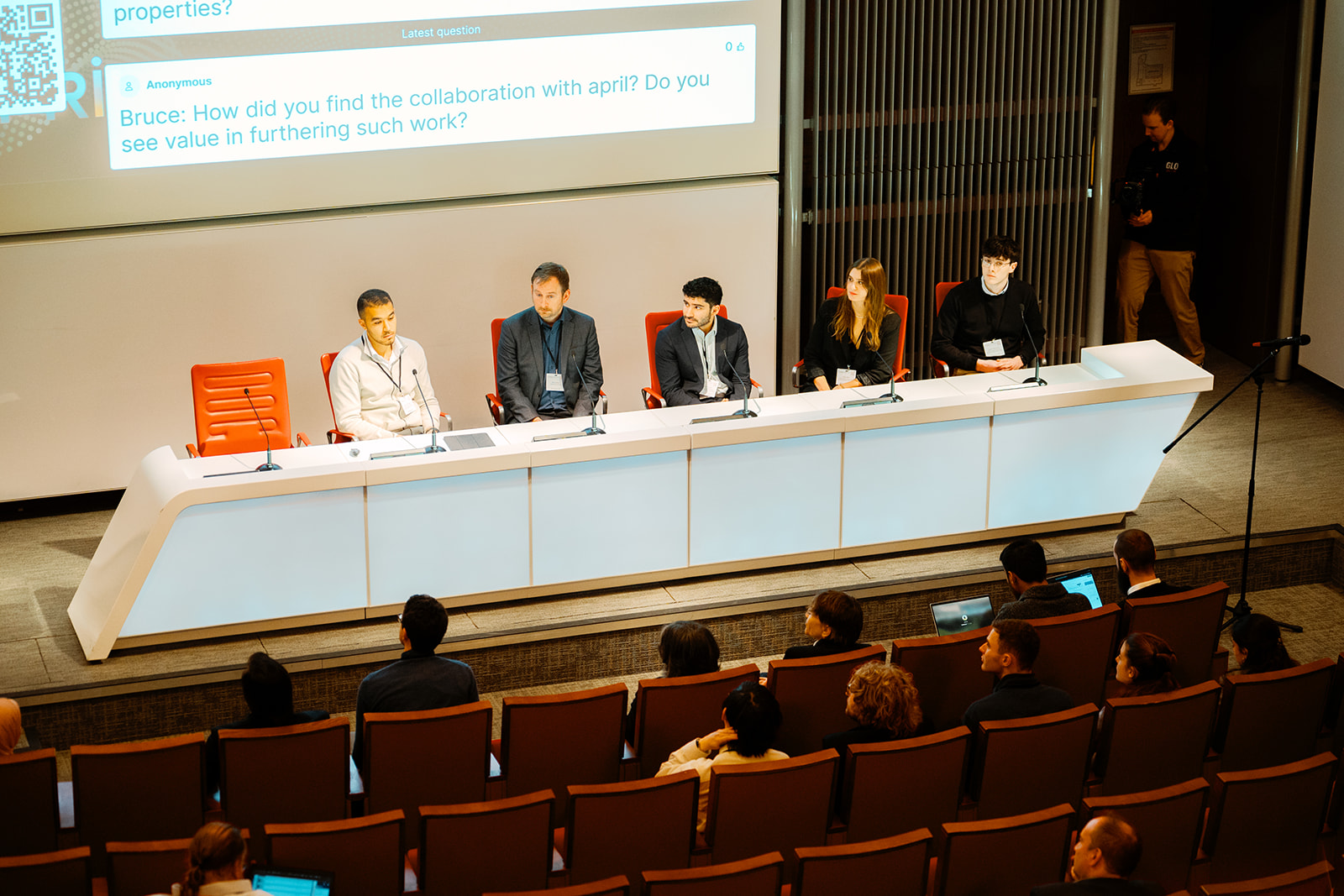
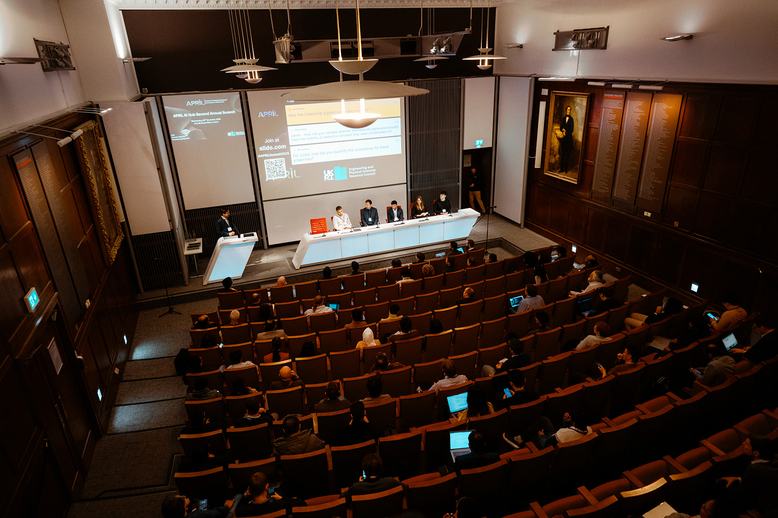
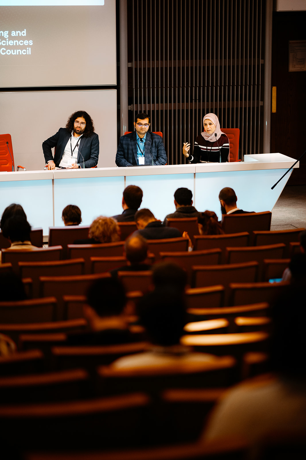
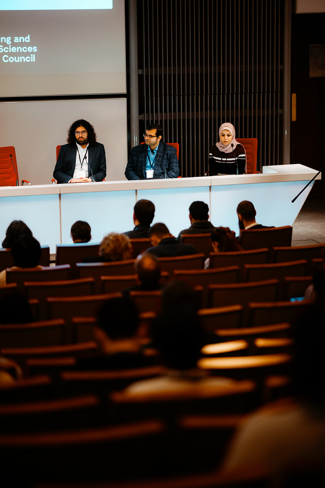
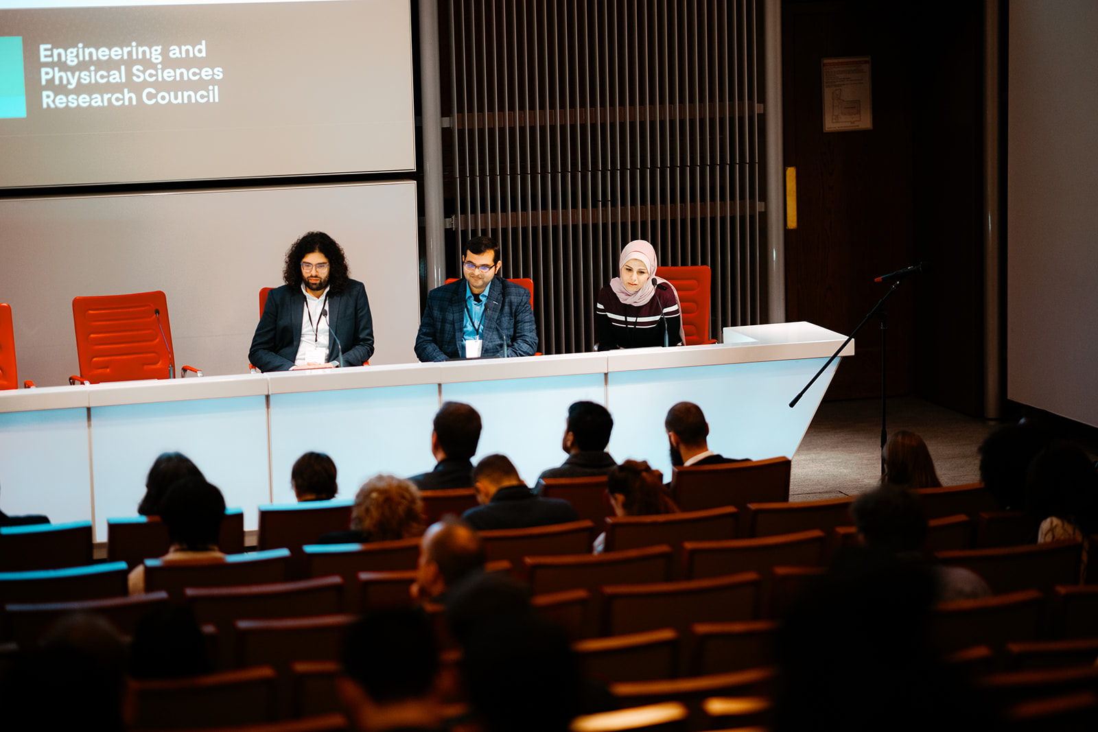
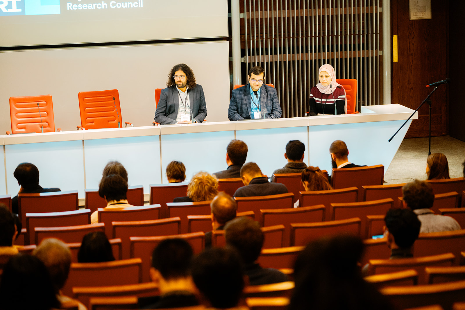
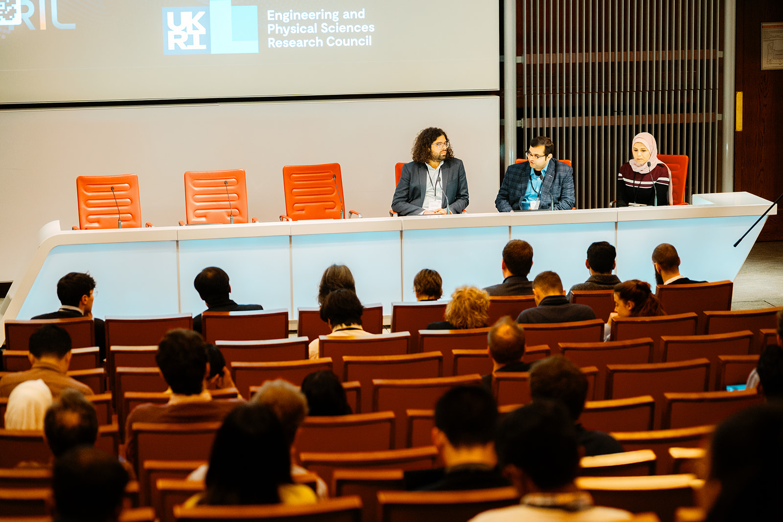
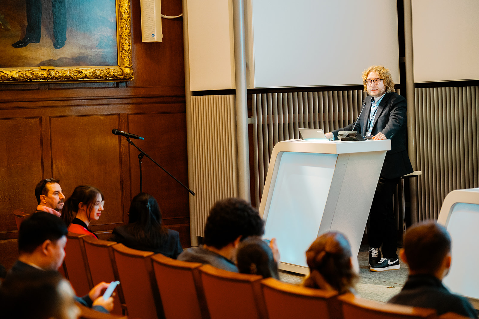
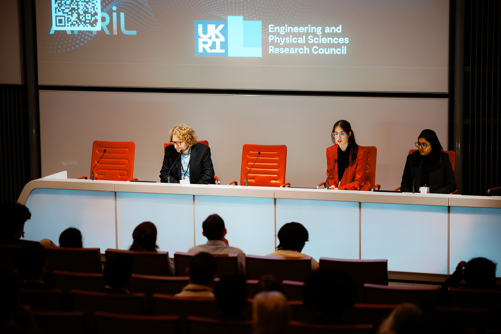
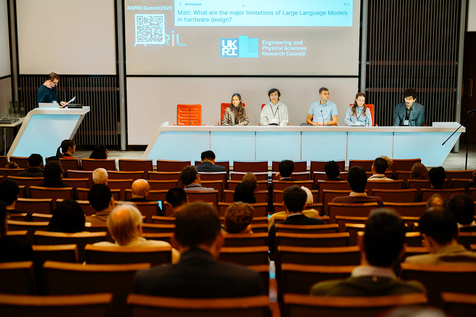
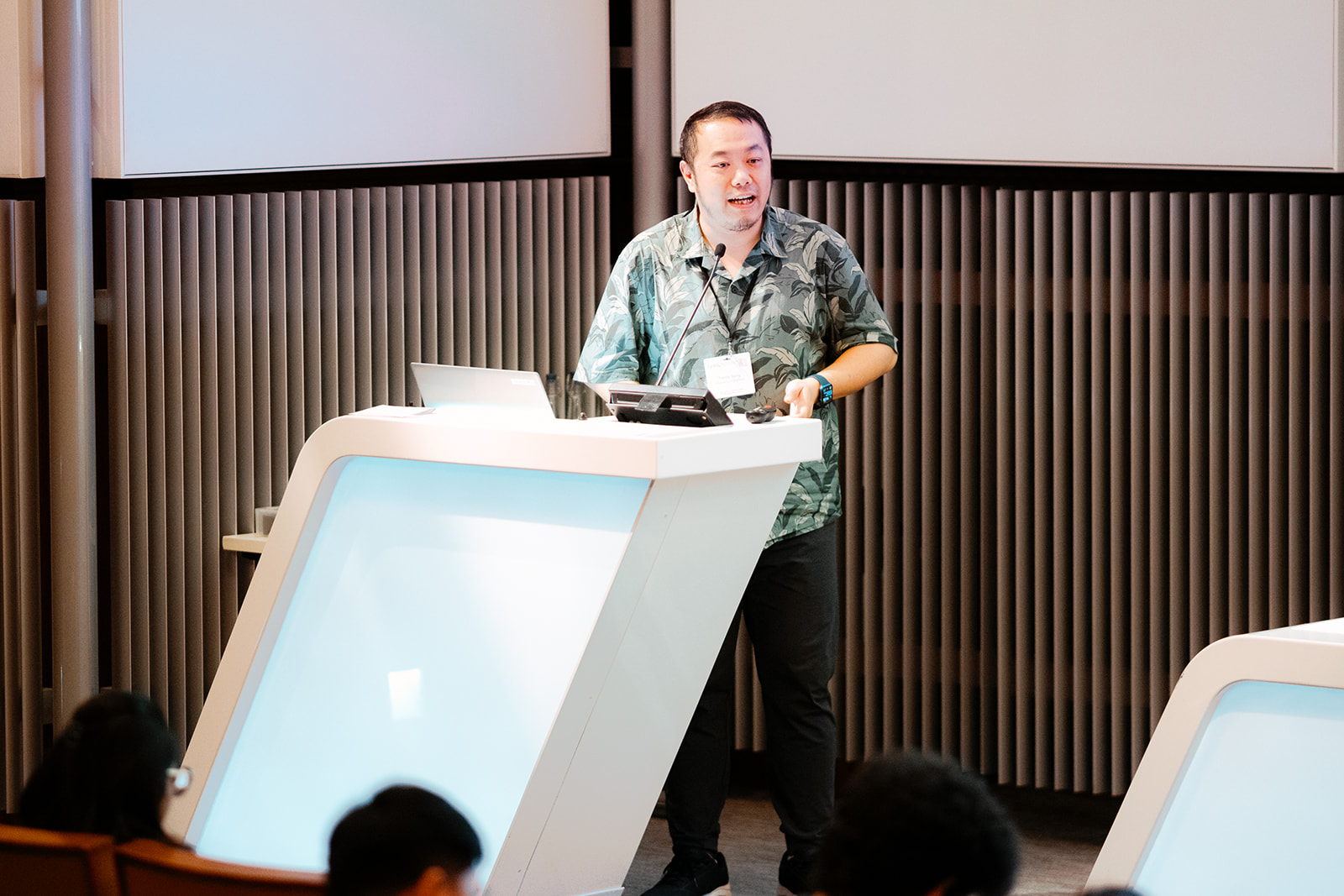
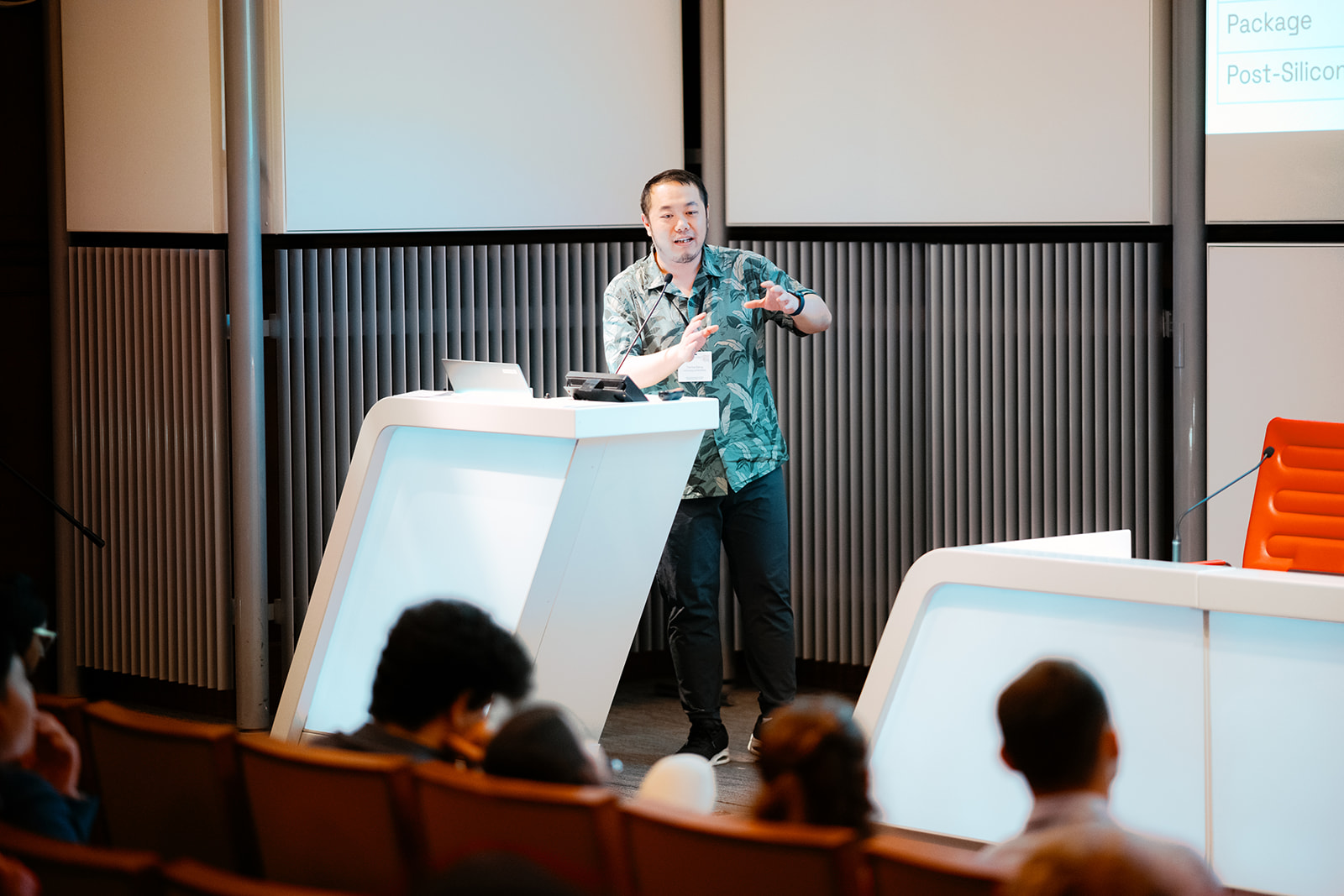
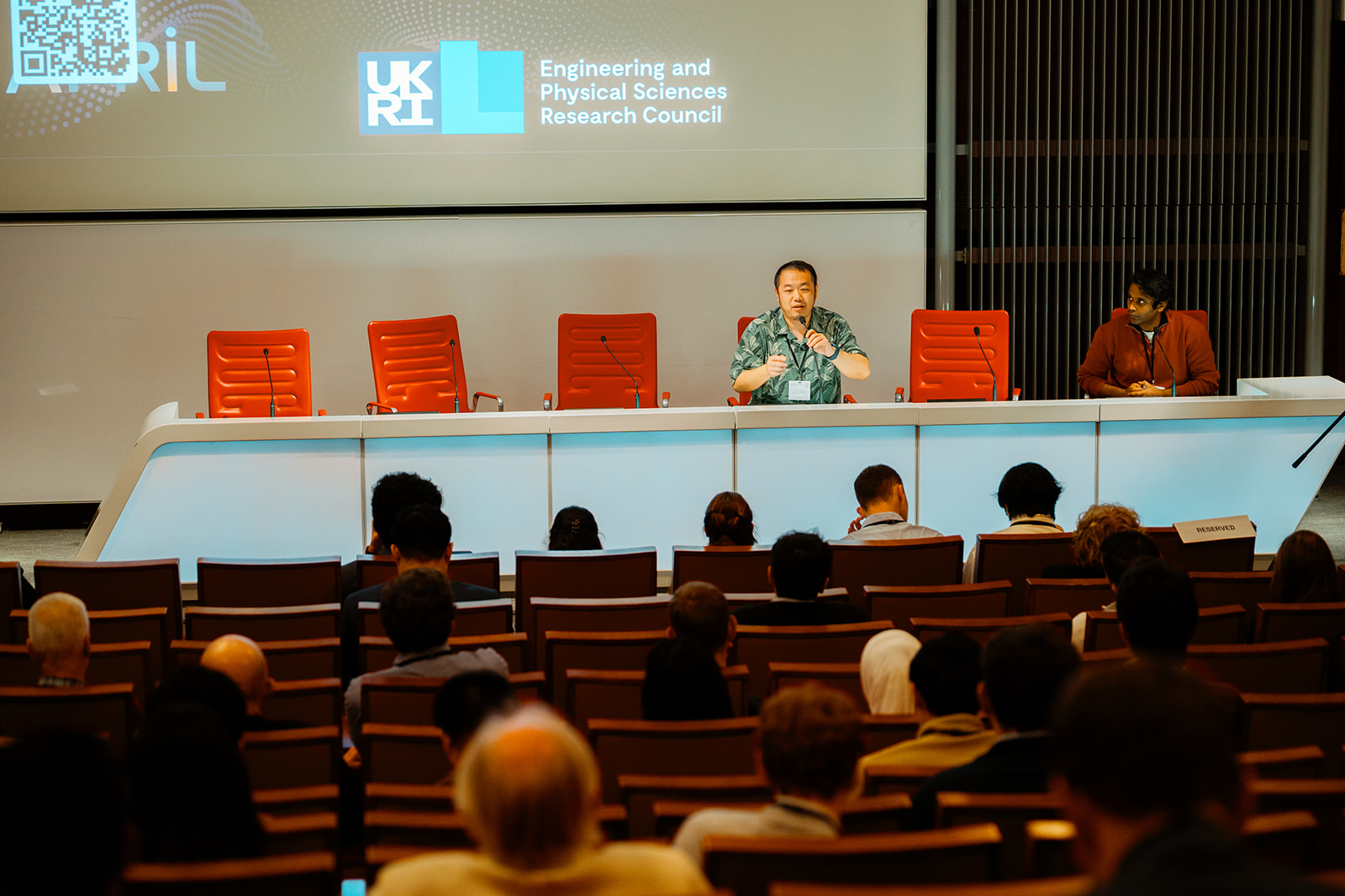
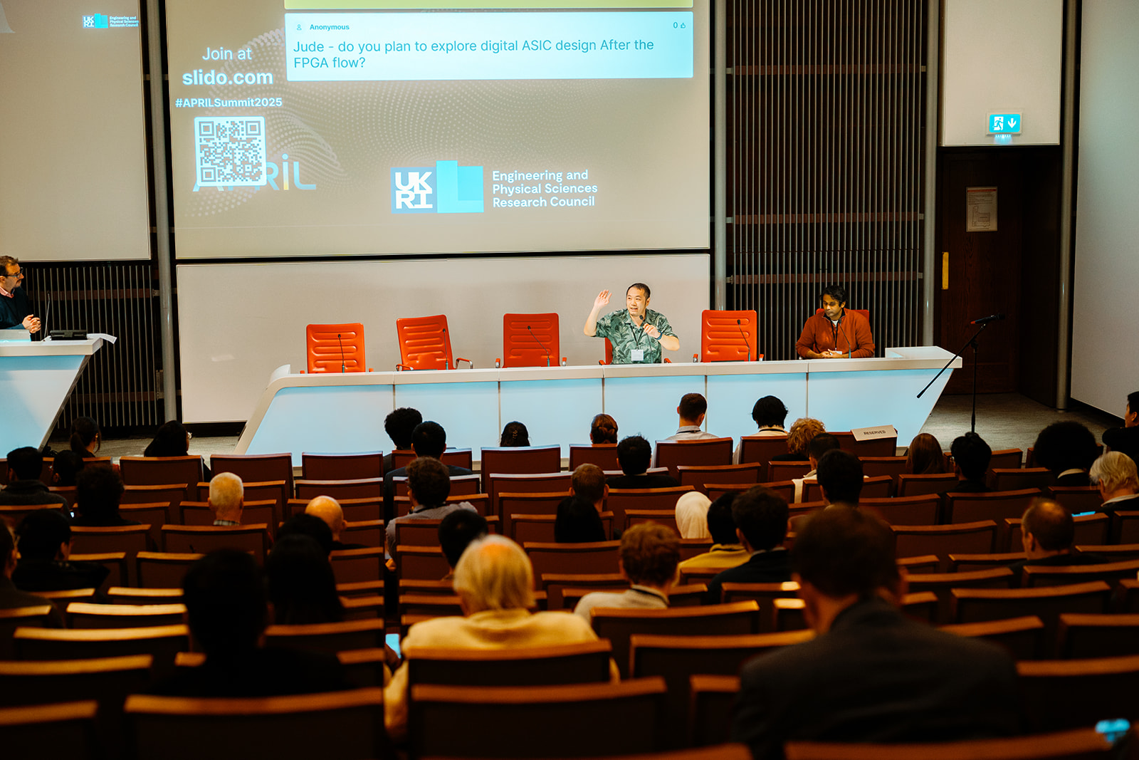
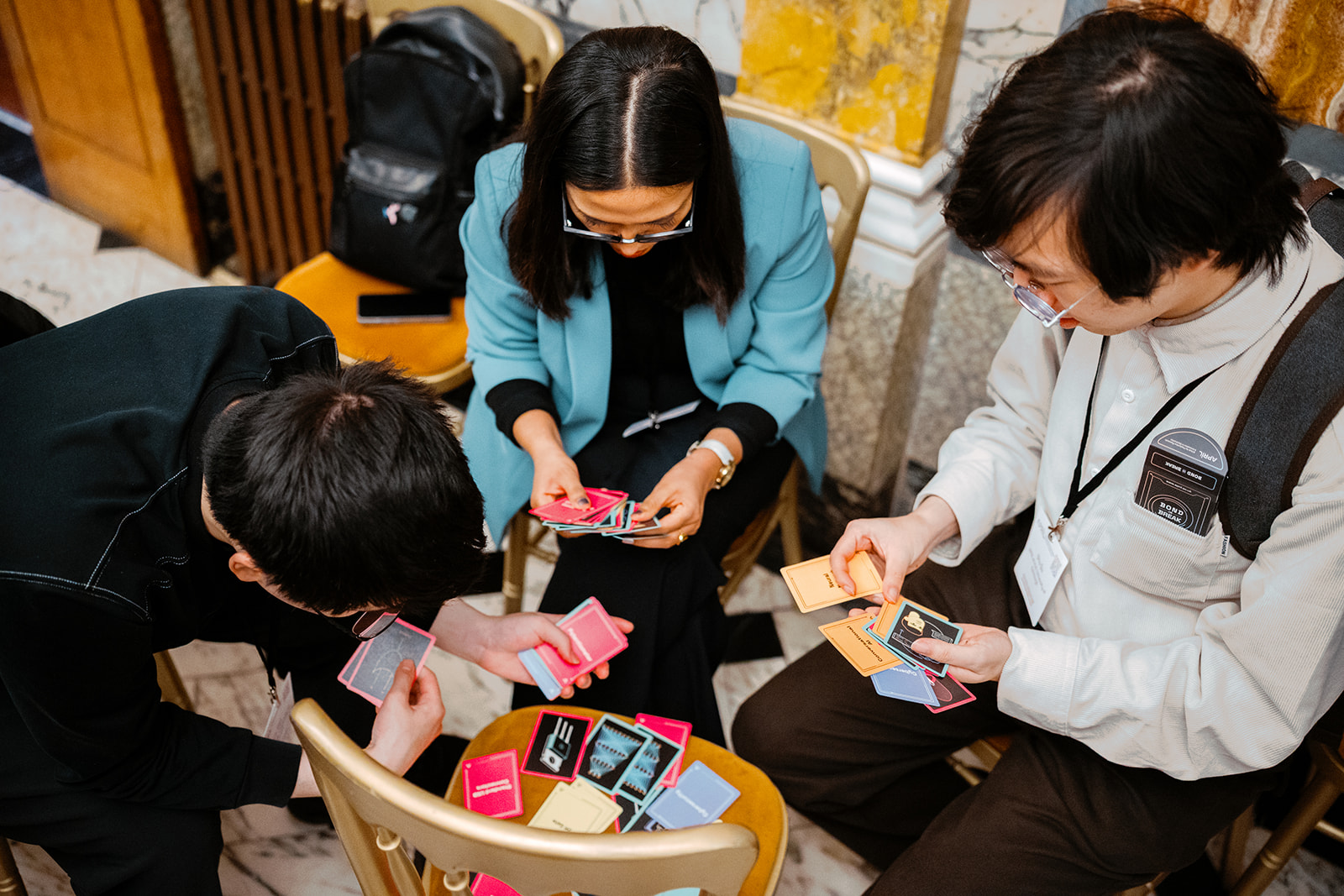
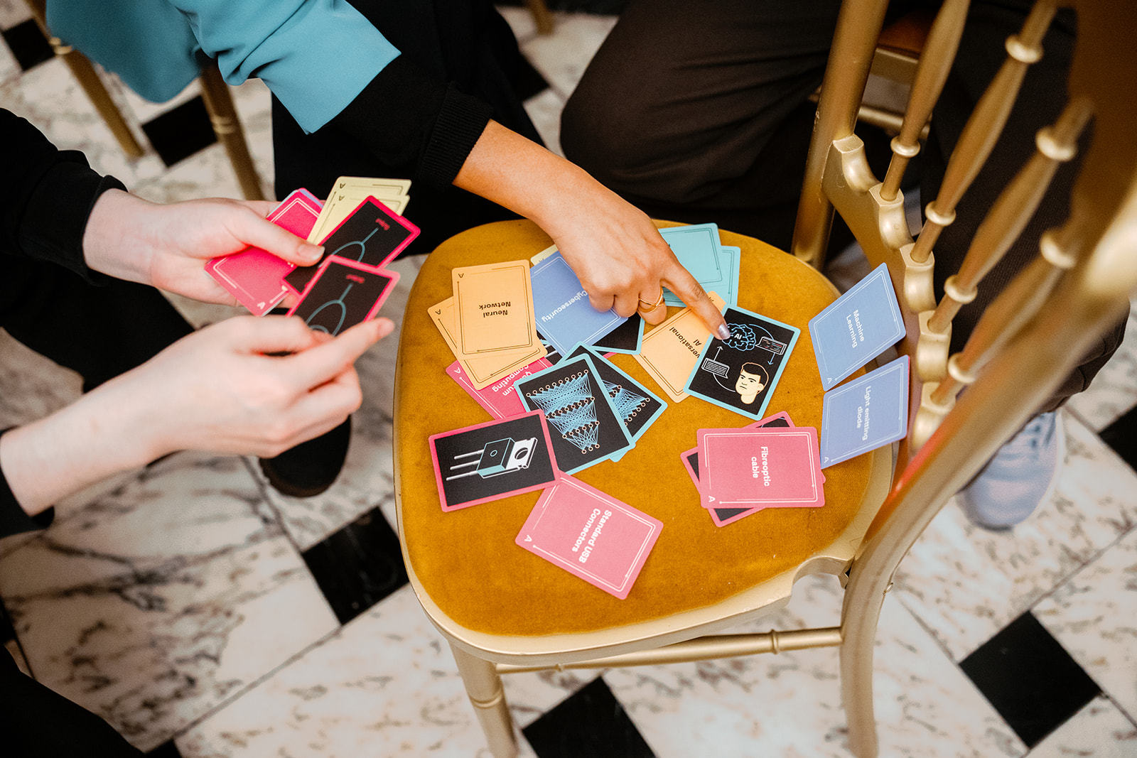
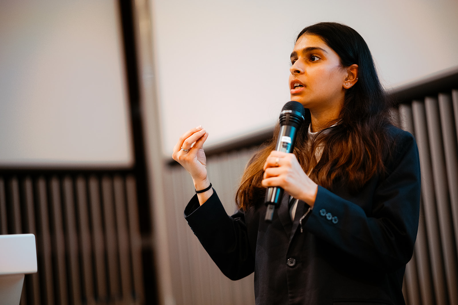
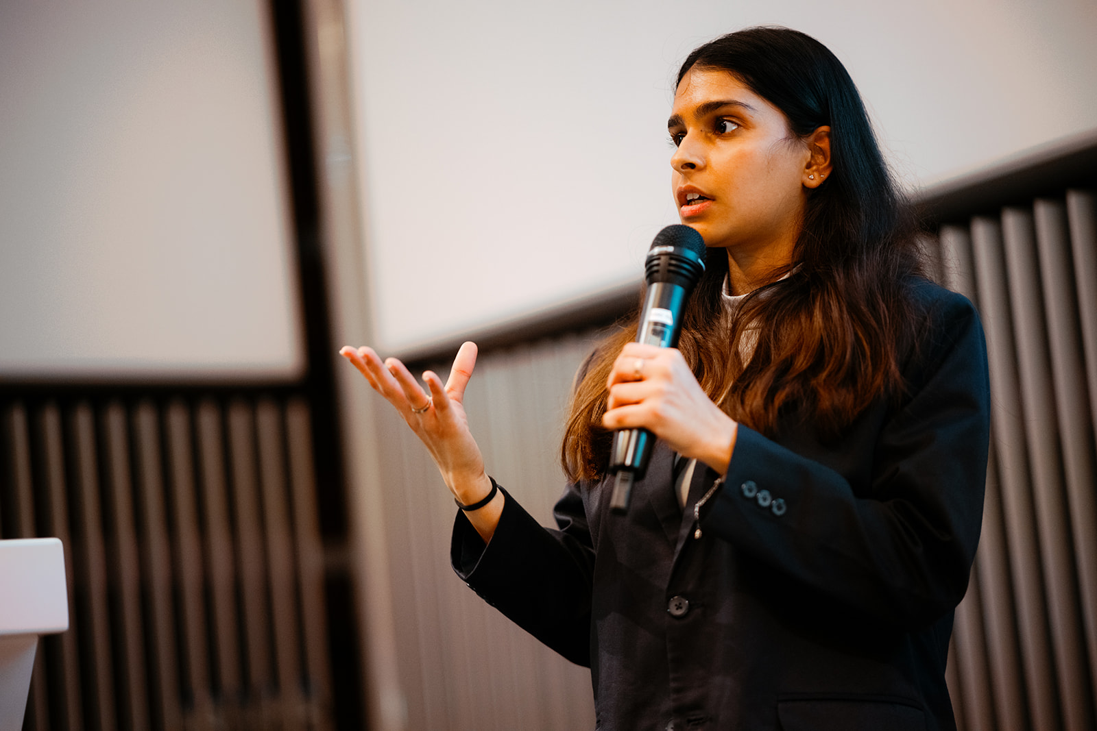
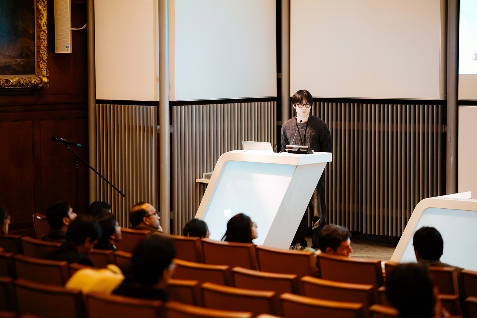
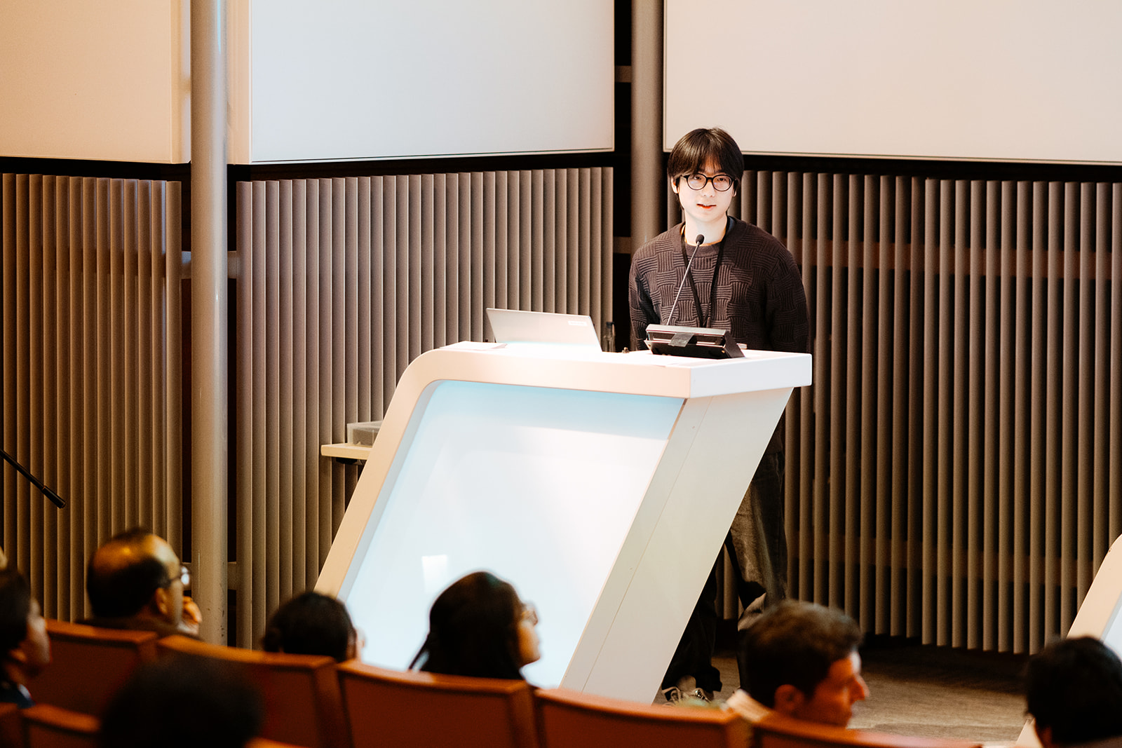
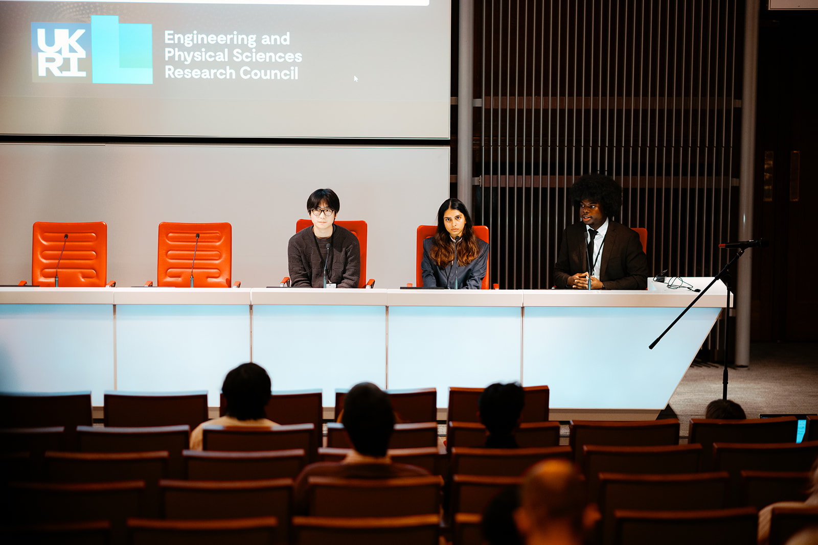
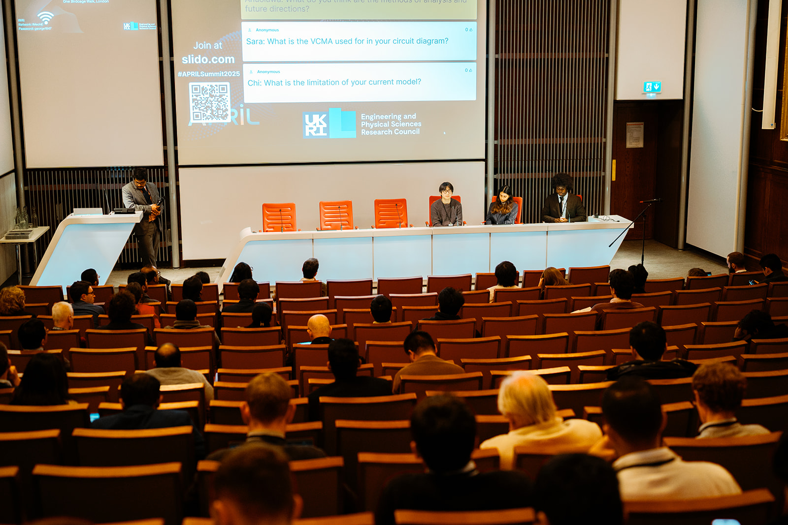
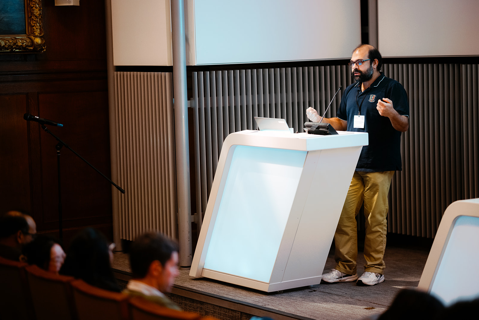
There will be panel discussions throughout the day focusing on: AI-Driven Materials Discovery and Device Design,AI-Driven Circuits Design Automation & Verification, and Machine Learning for CMOS and Beyond CMOS Devices Design. There will also be poster sessions & demos presented by our community.
Download our leaflet here to share with peers and colleagues.
Itinerary:
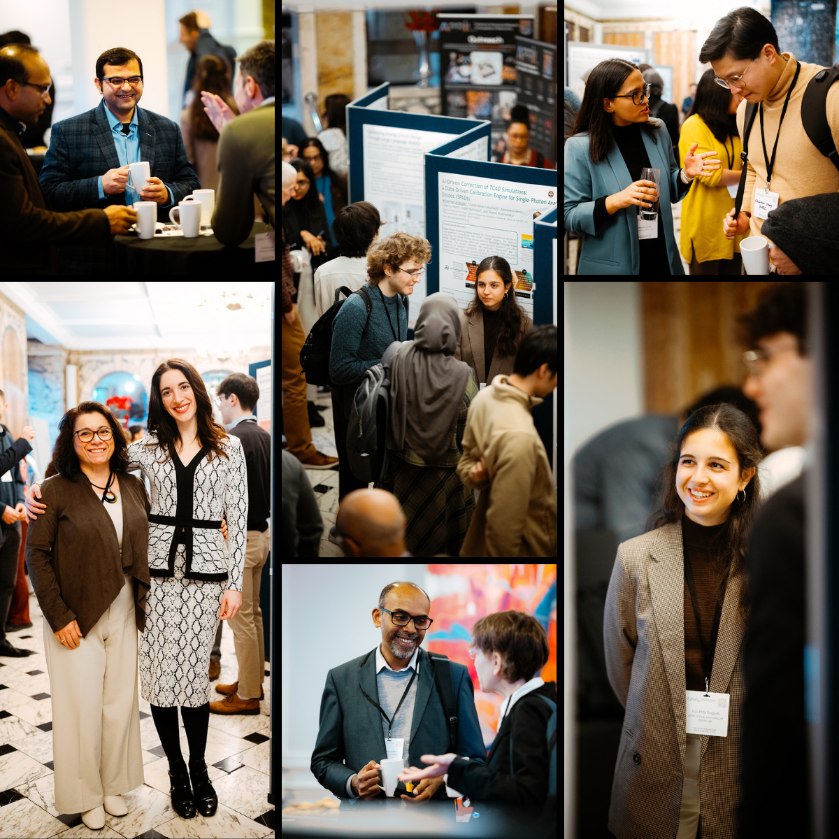
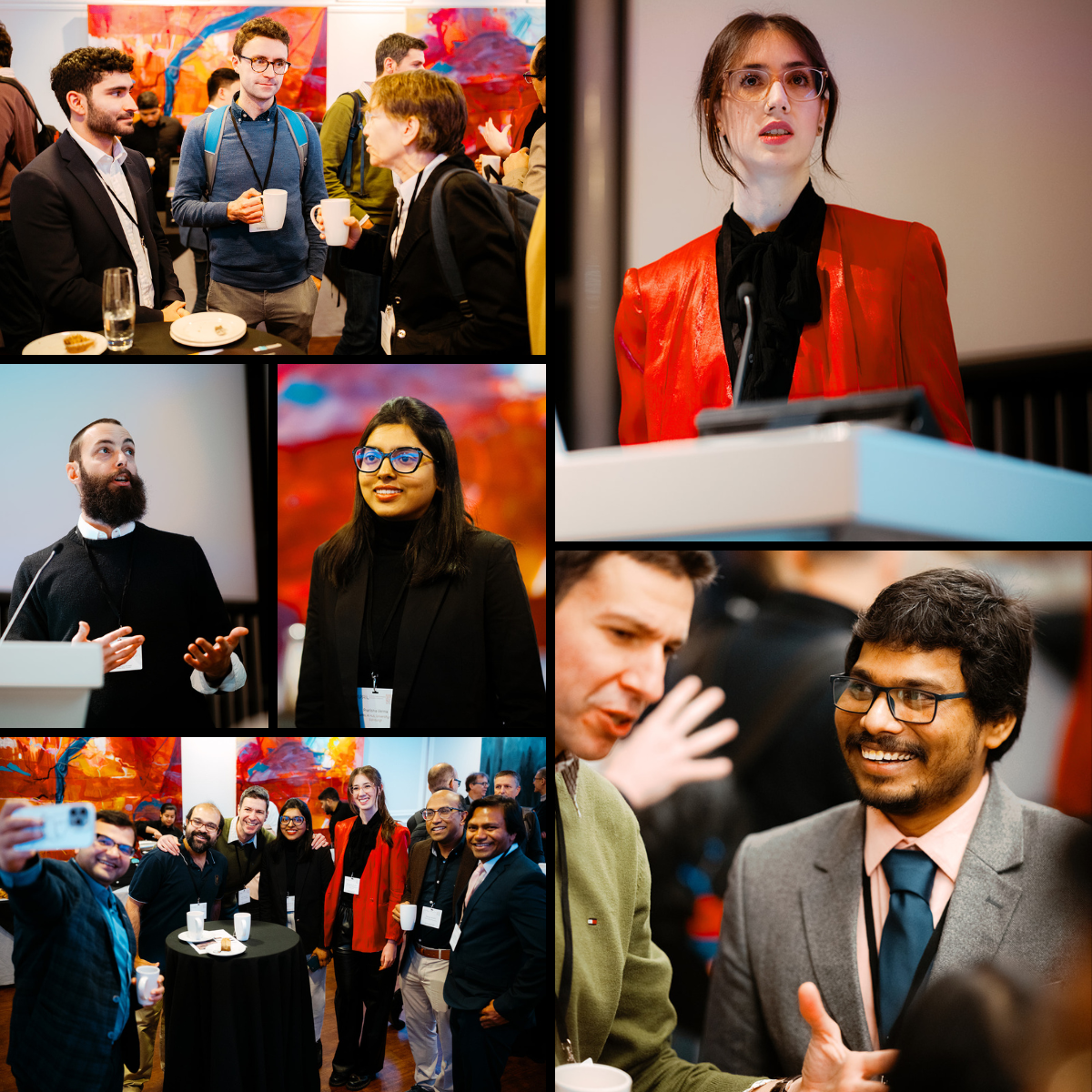
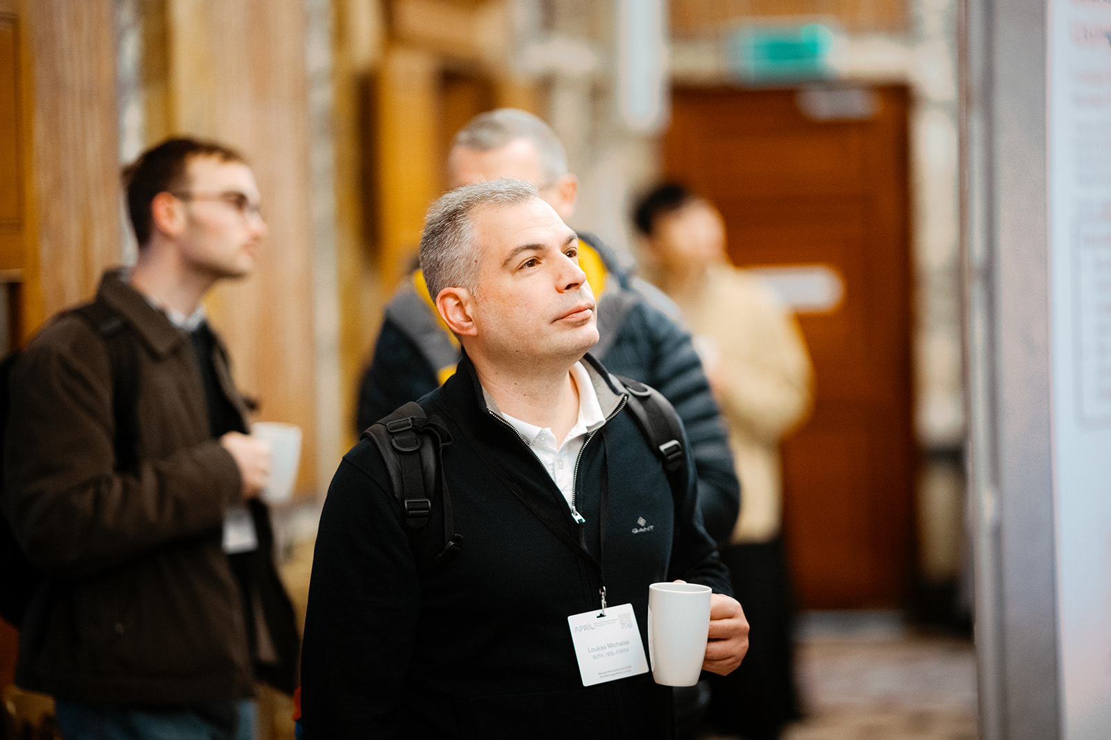
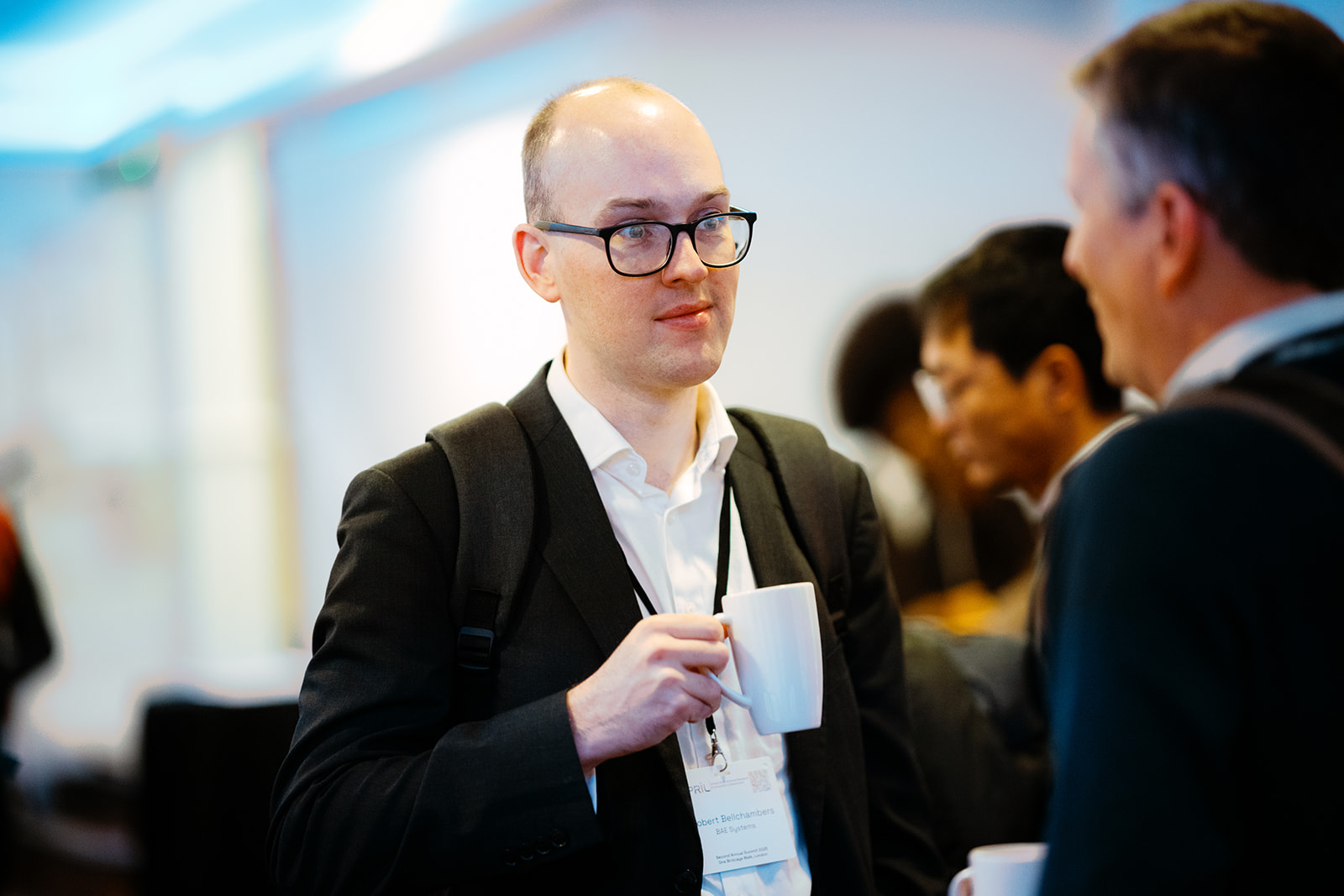
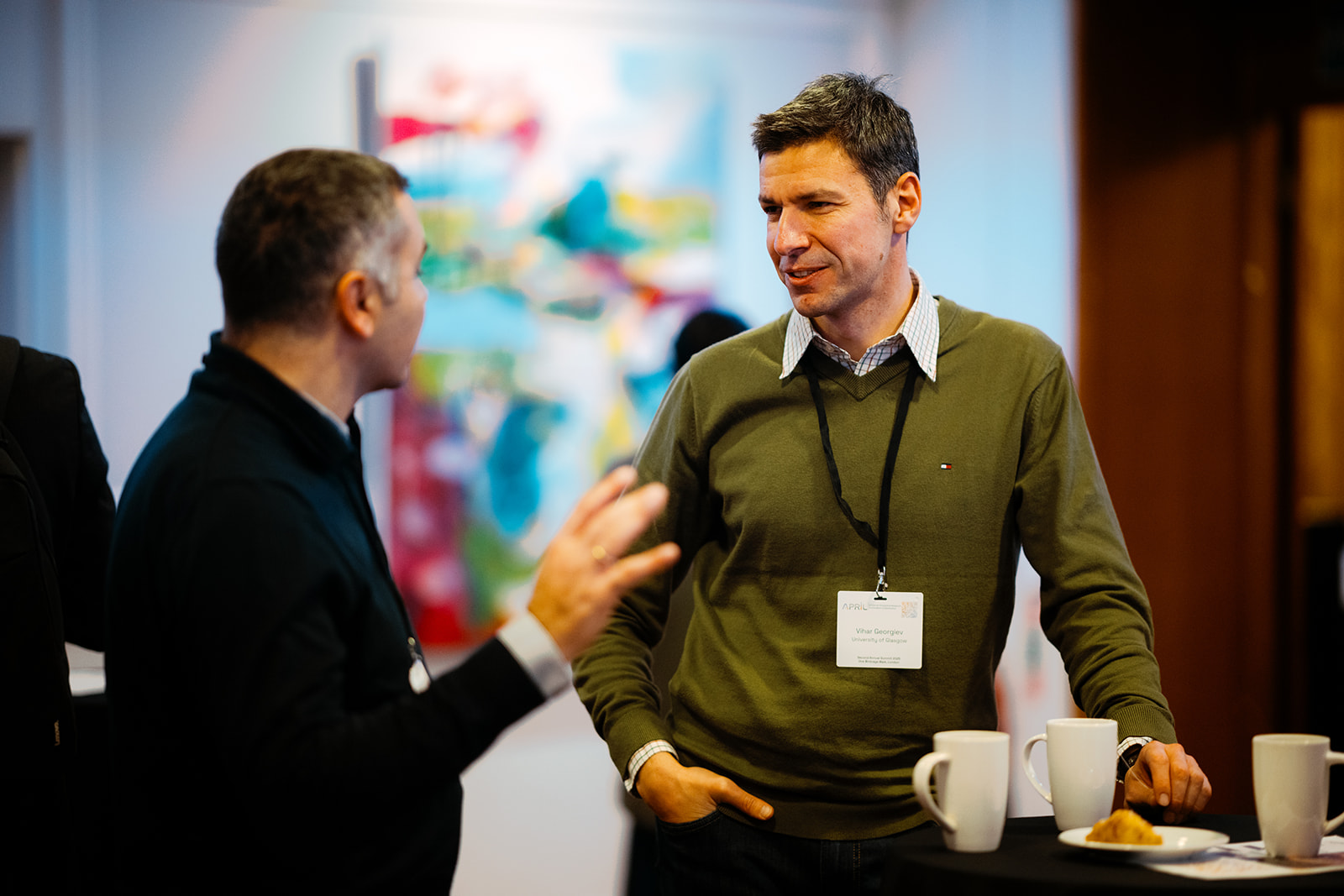
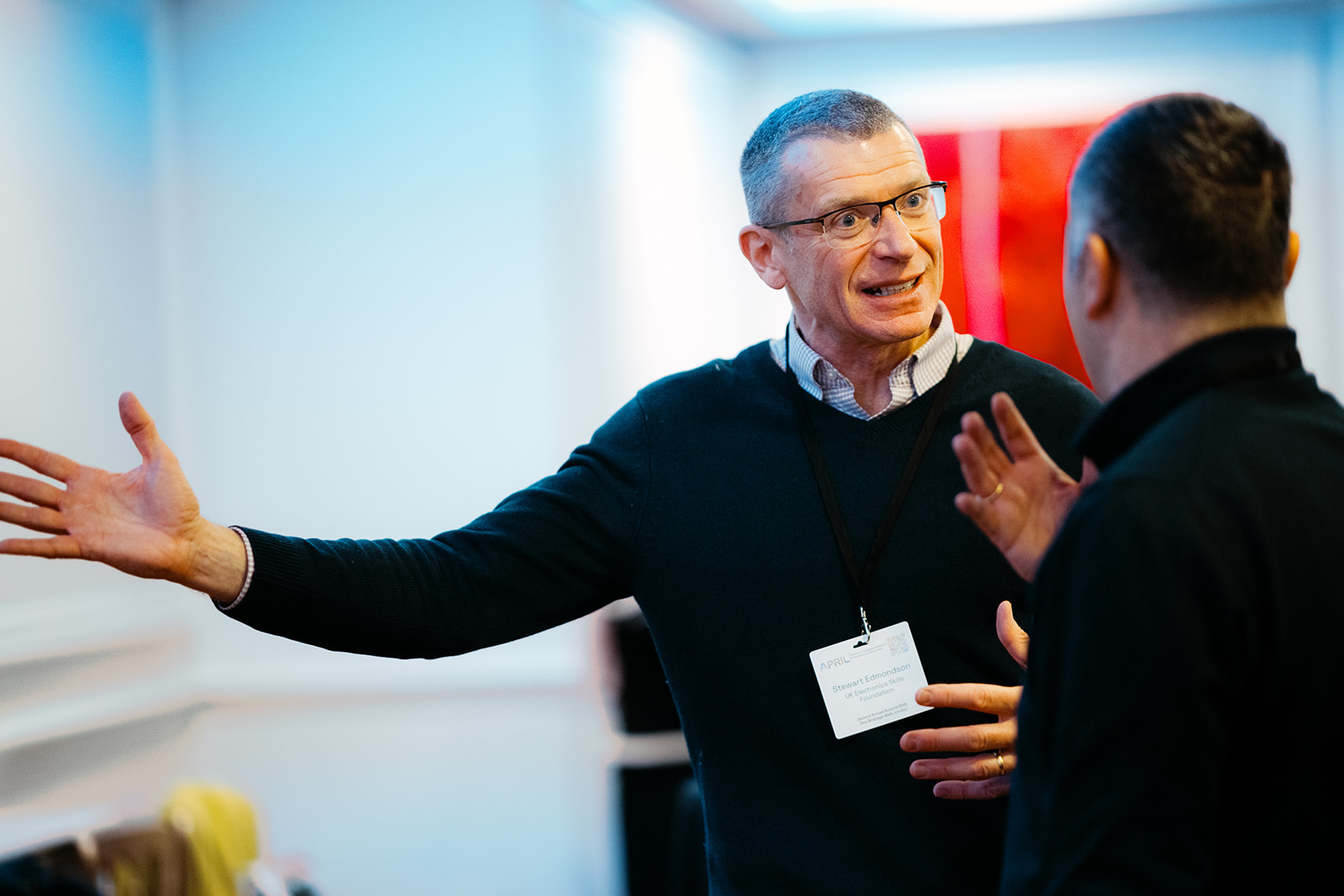
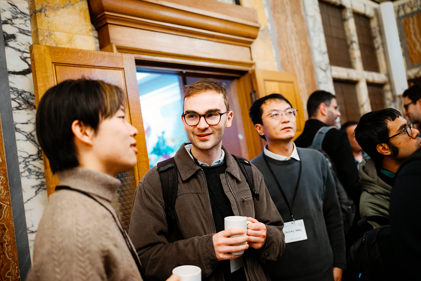
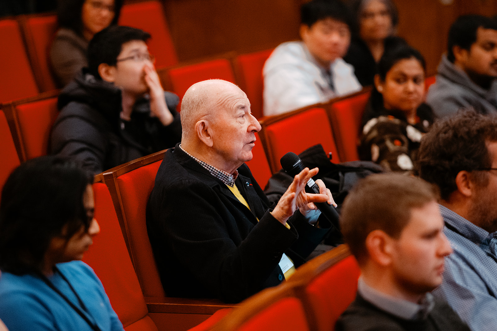
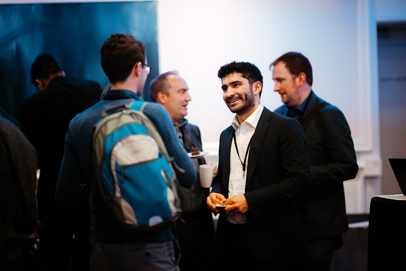
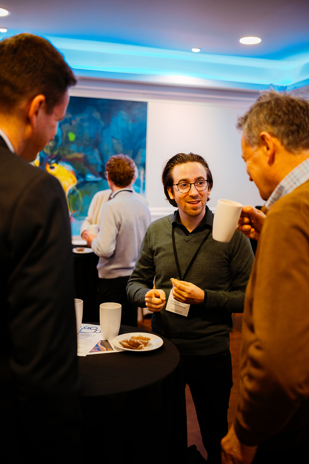
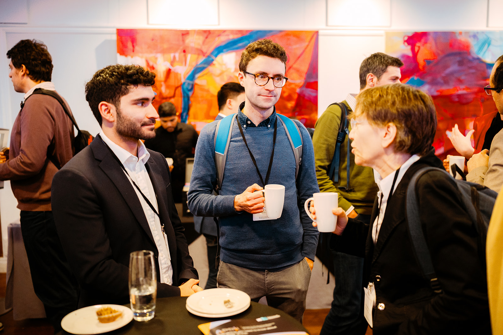
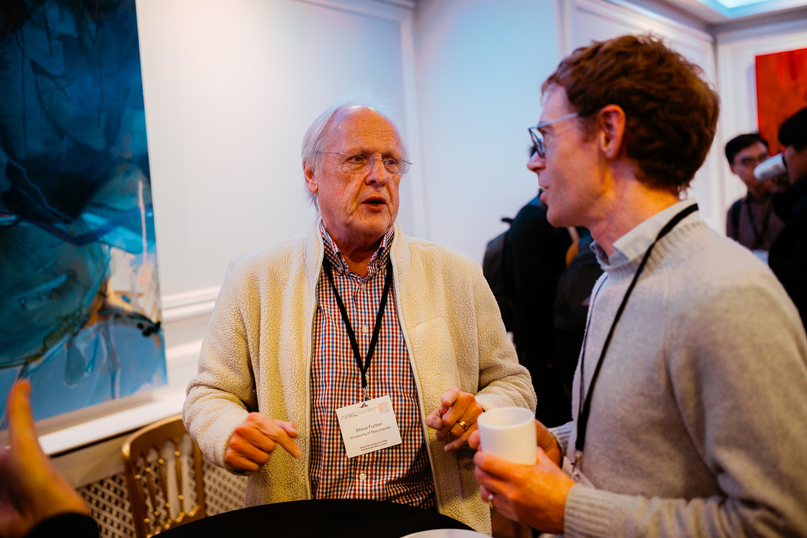
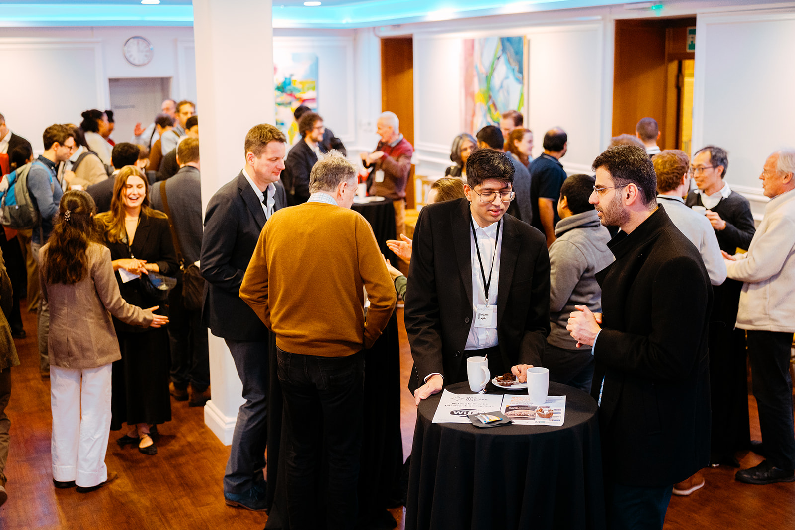
9:30 – 10:30 – Registration & Refreshments
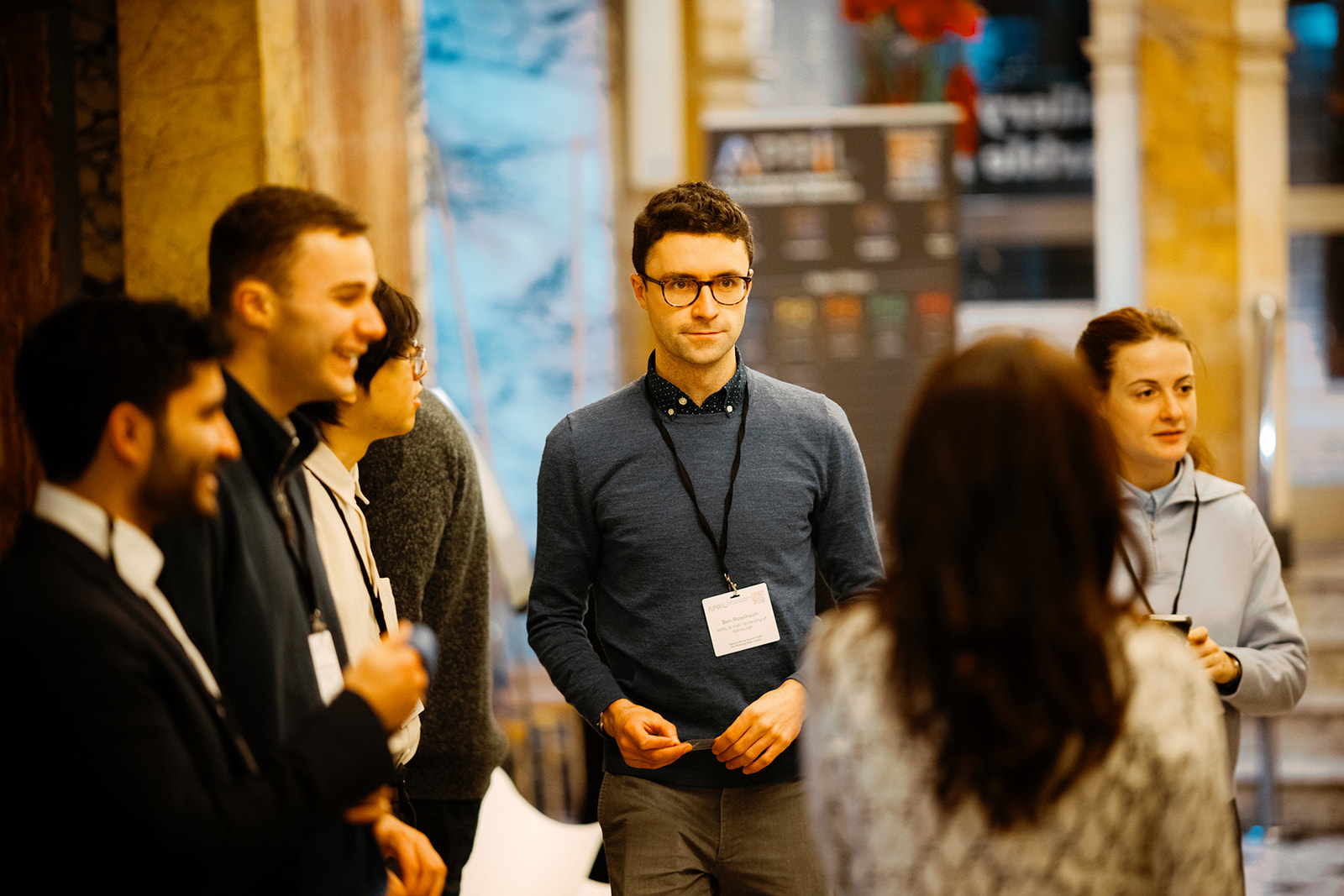
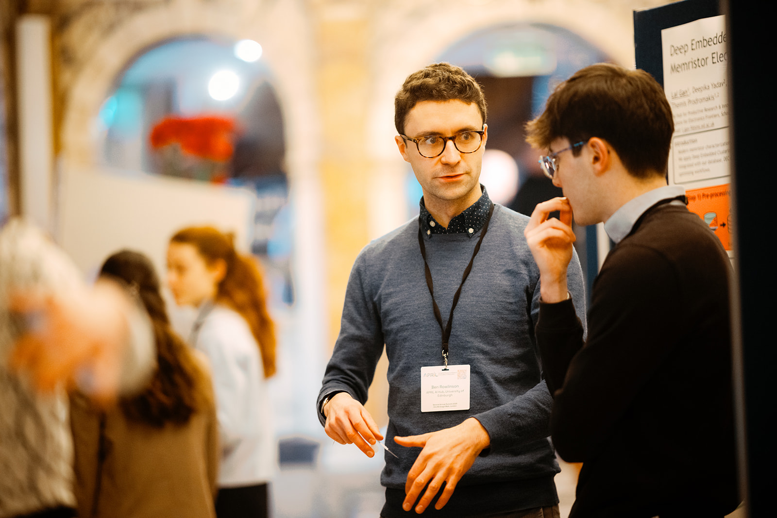
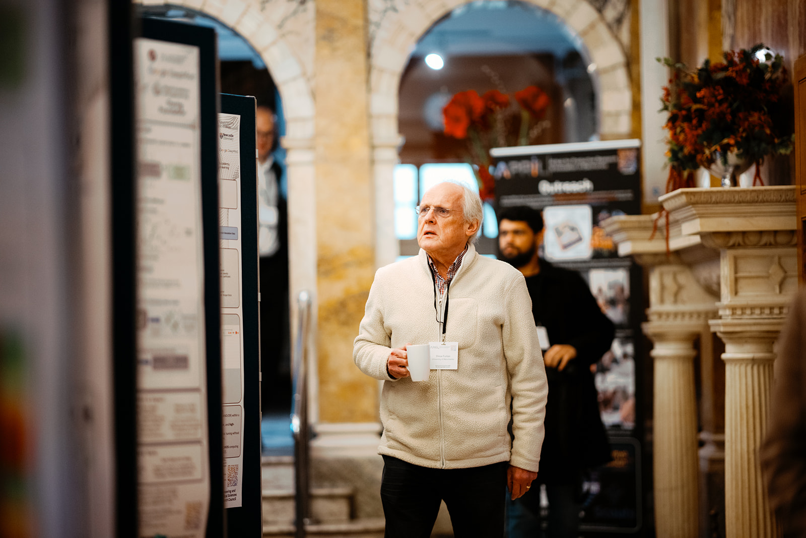
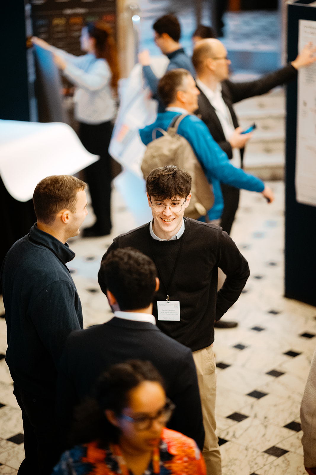
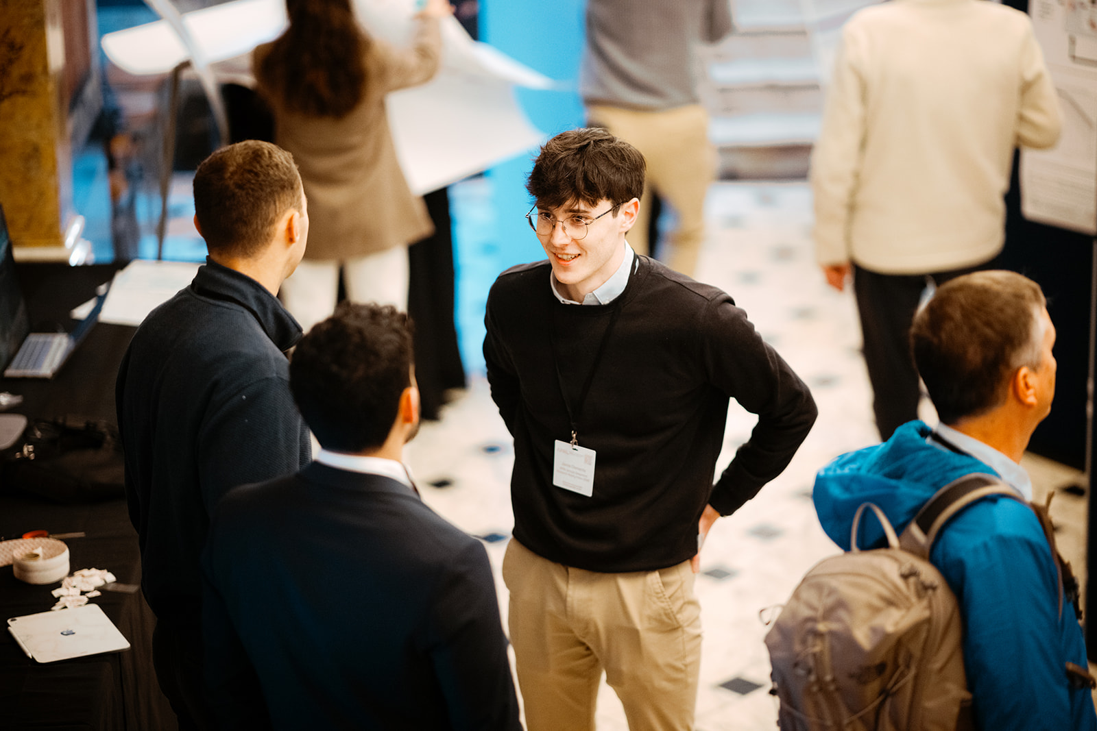
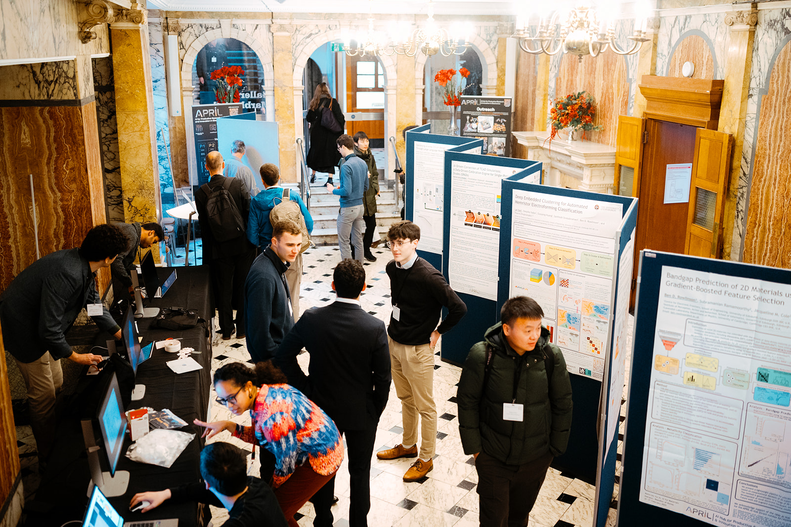
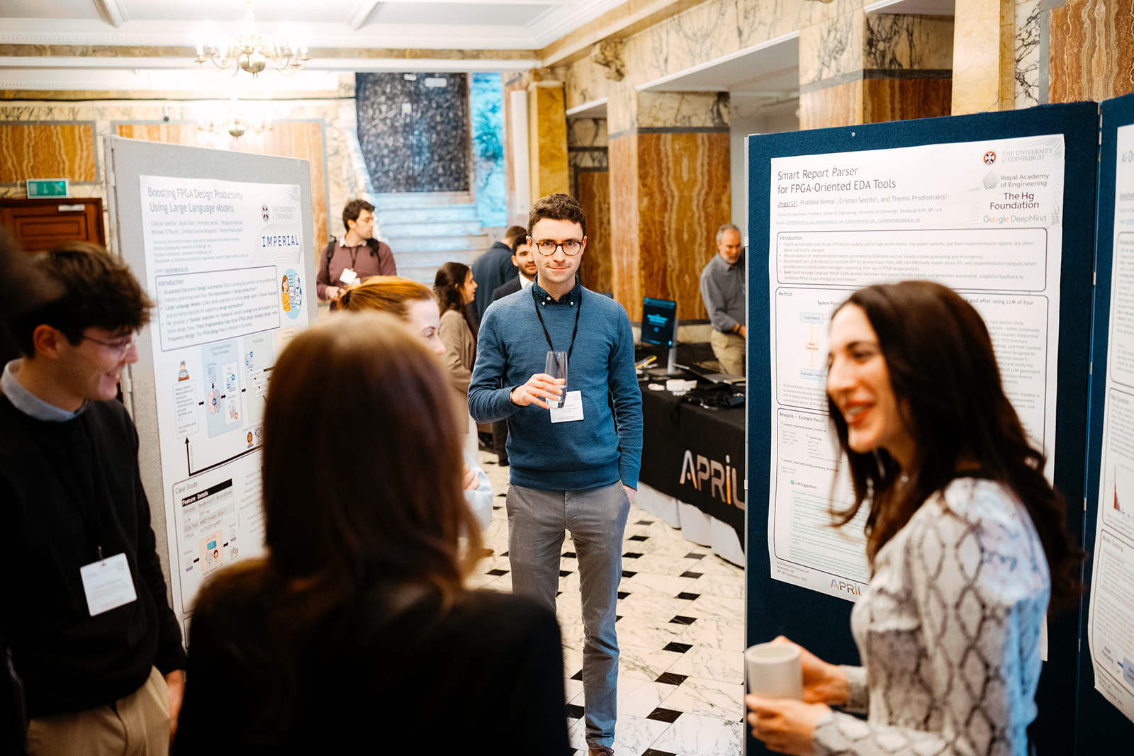
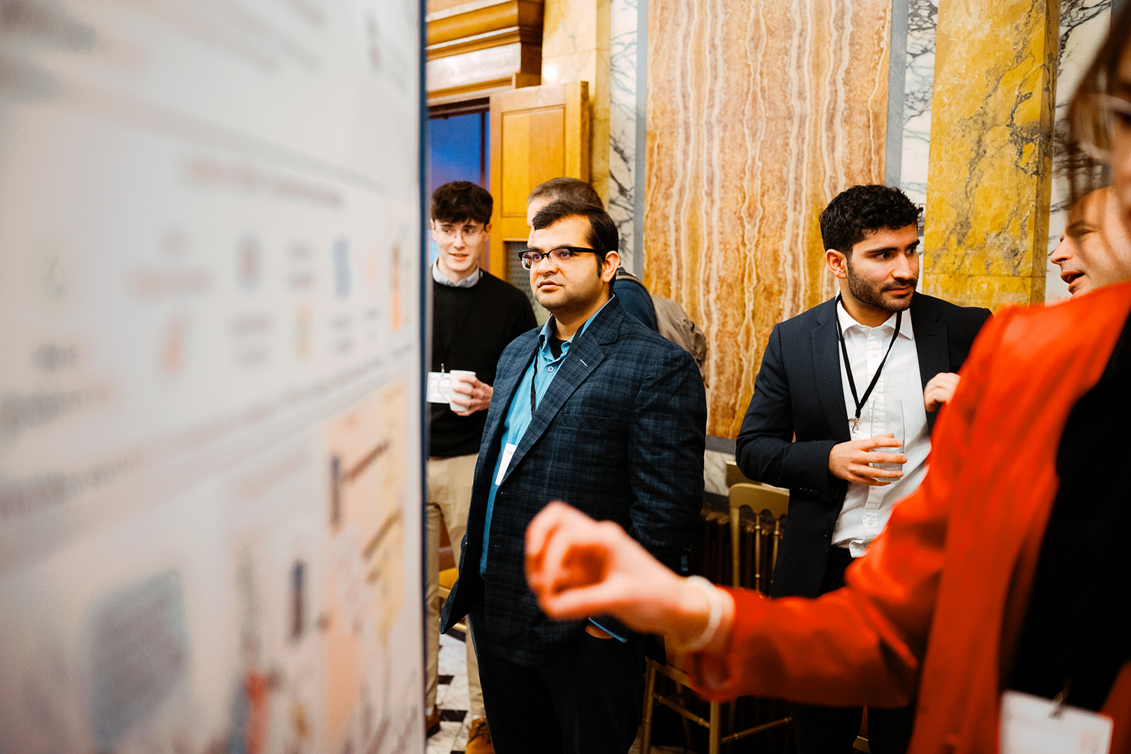
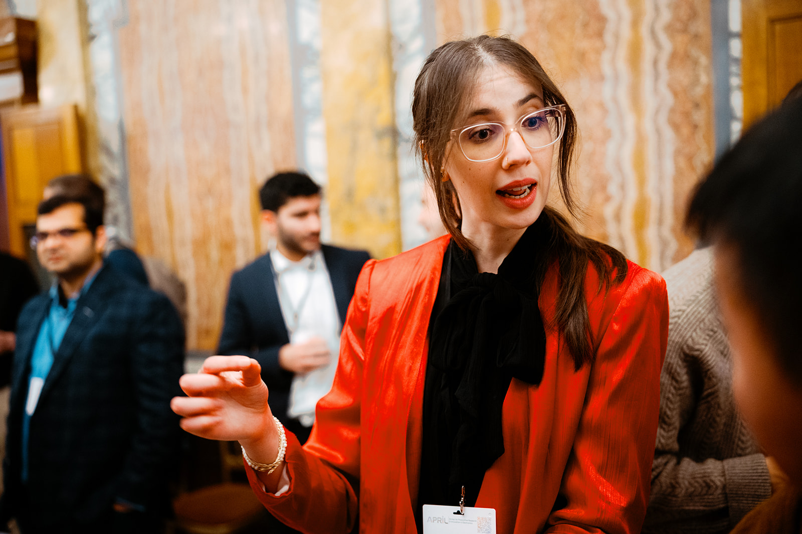
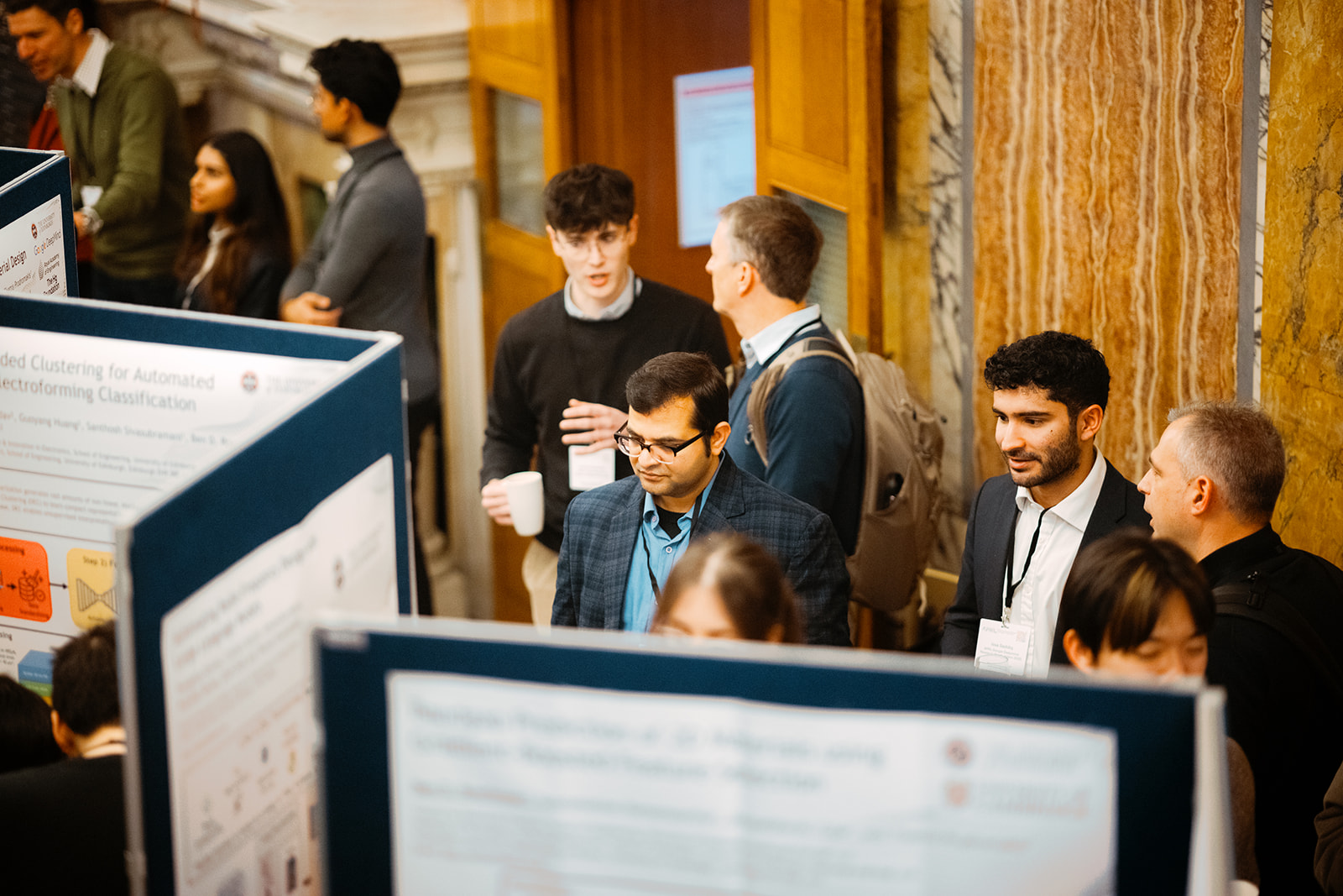
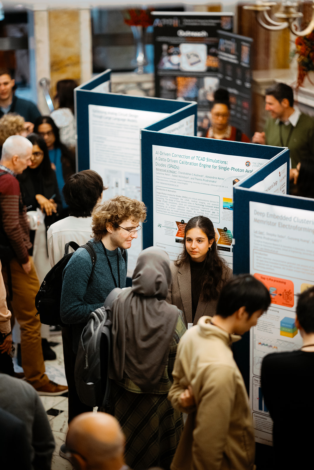
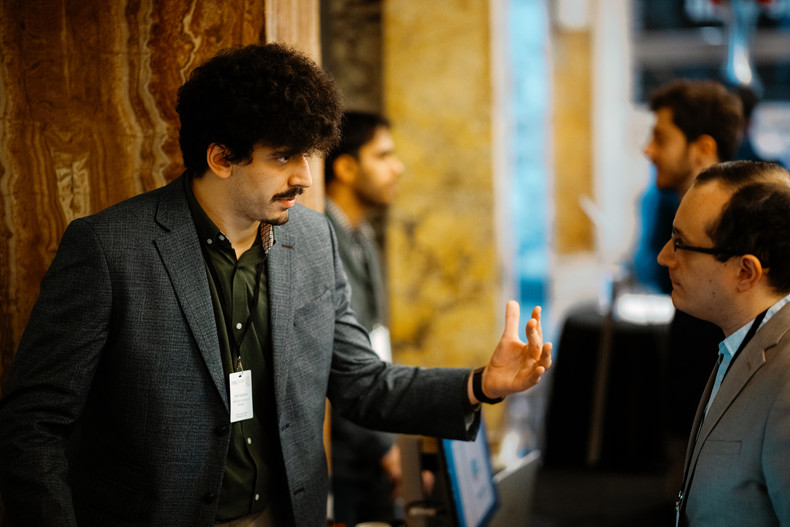
10:00 – 11:00 – Poster & Demo Session
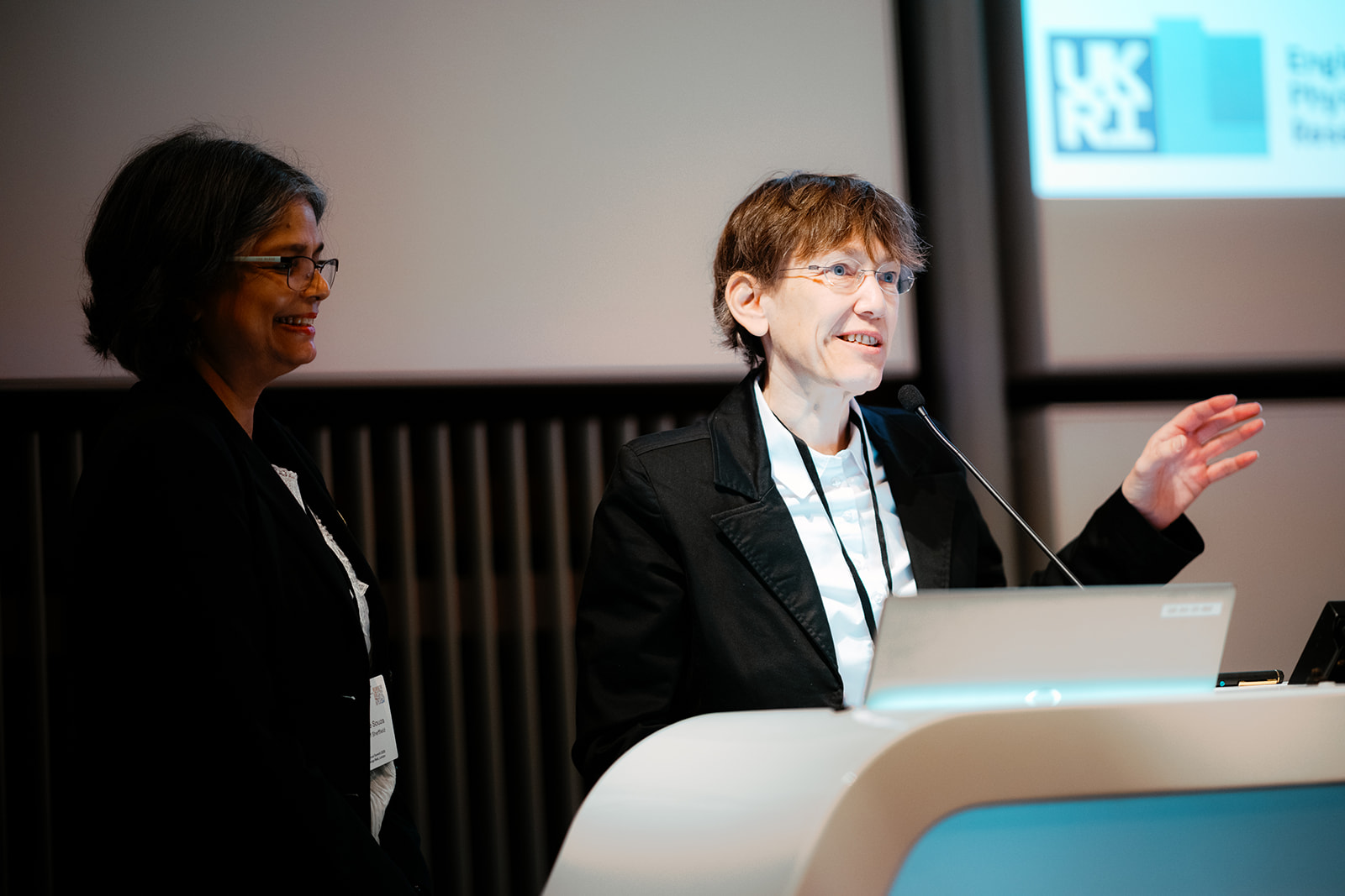
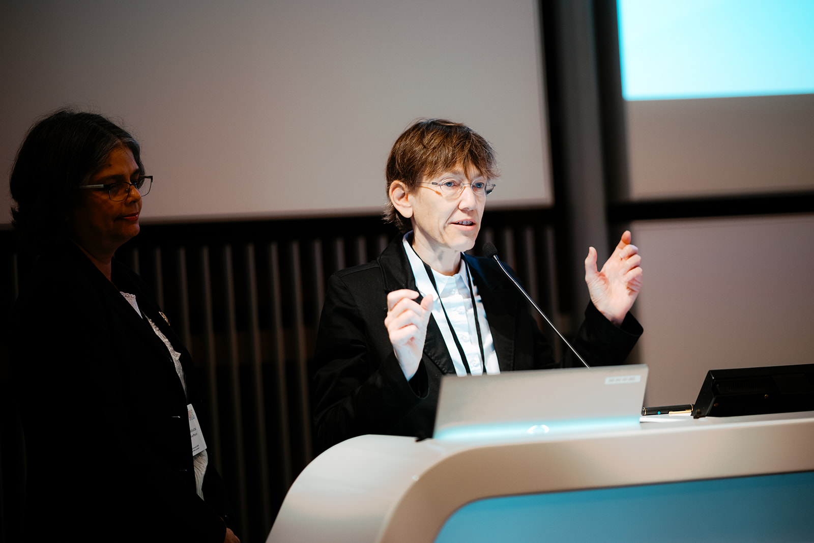
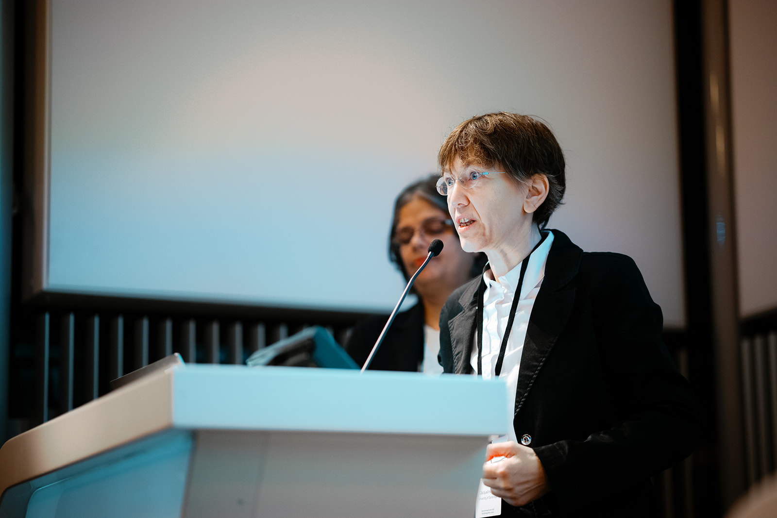
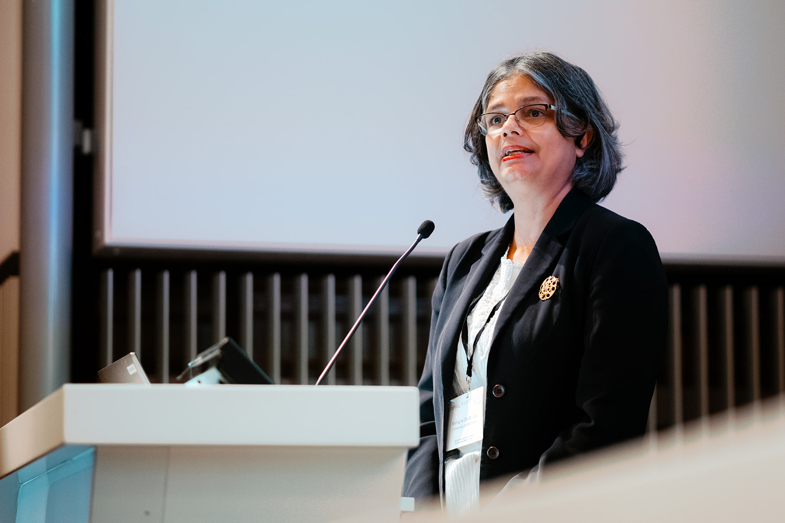
11:00 – 11:15 - Welcome
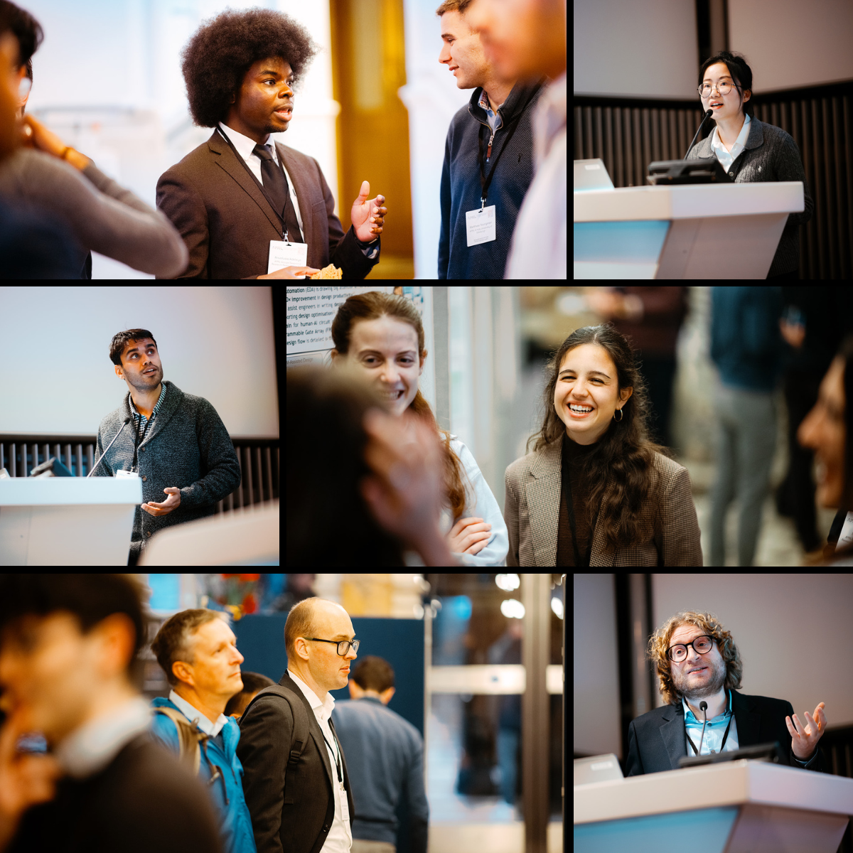
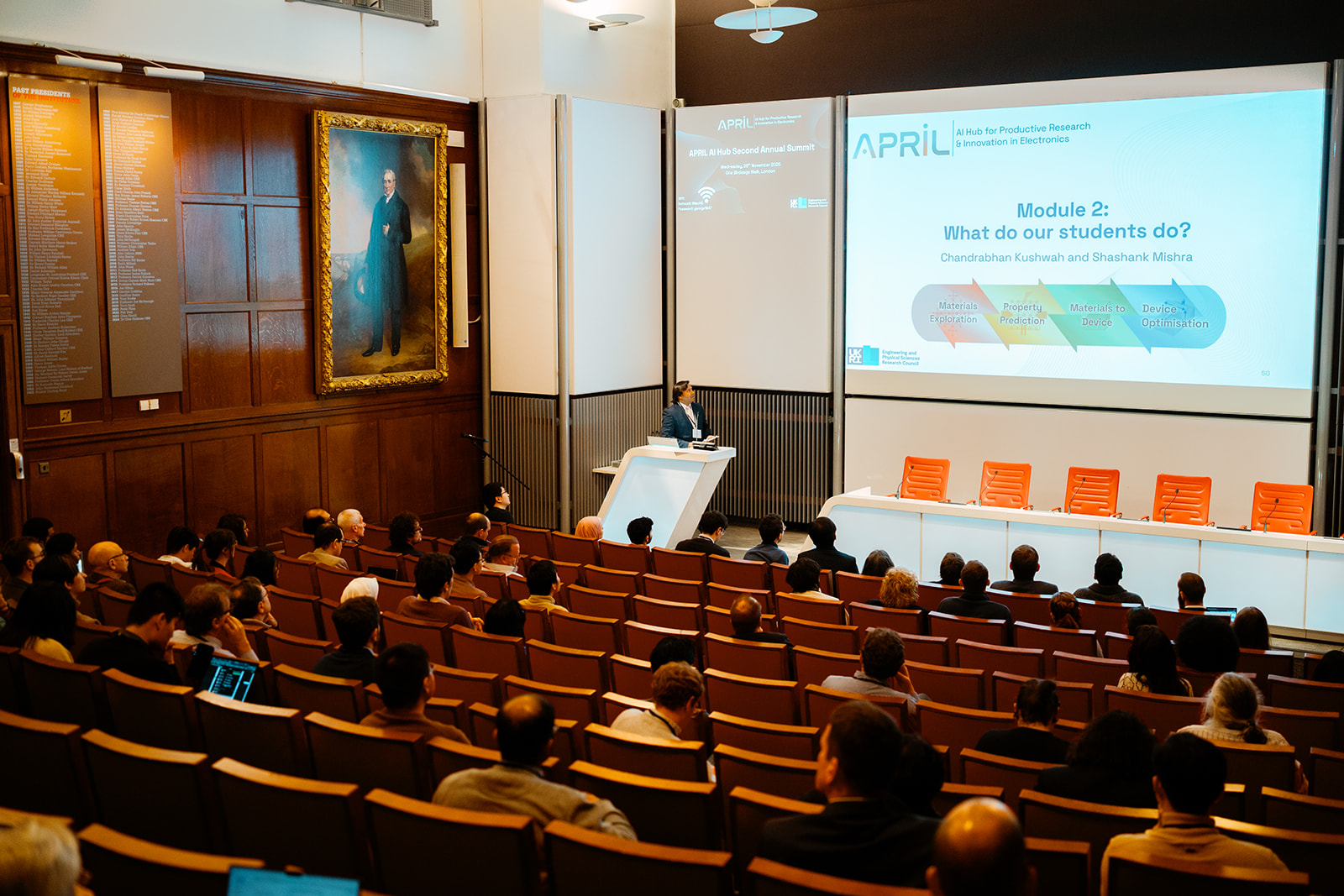
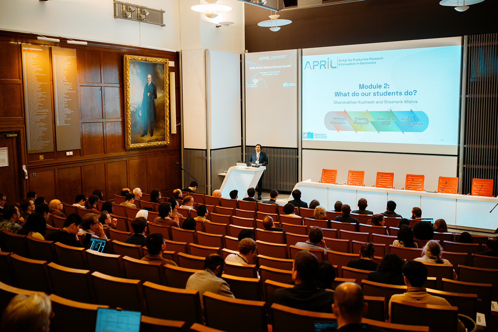
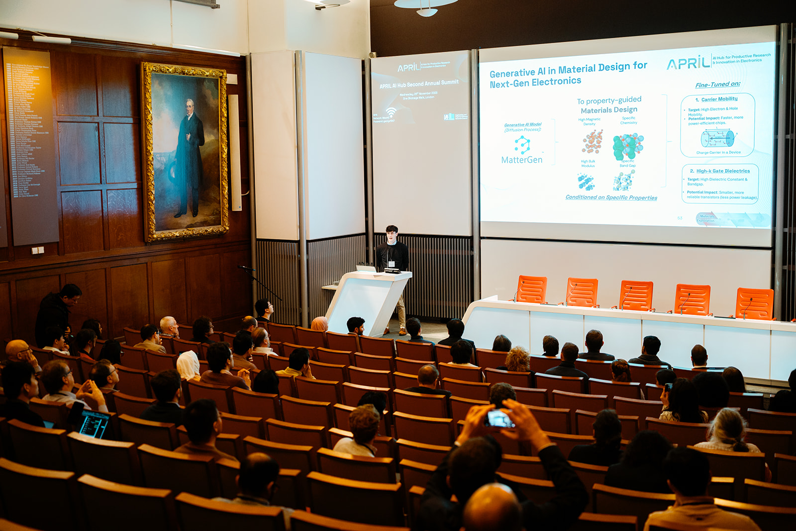
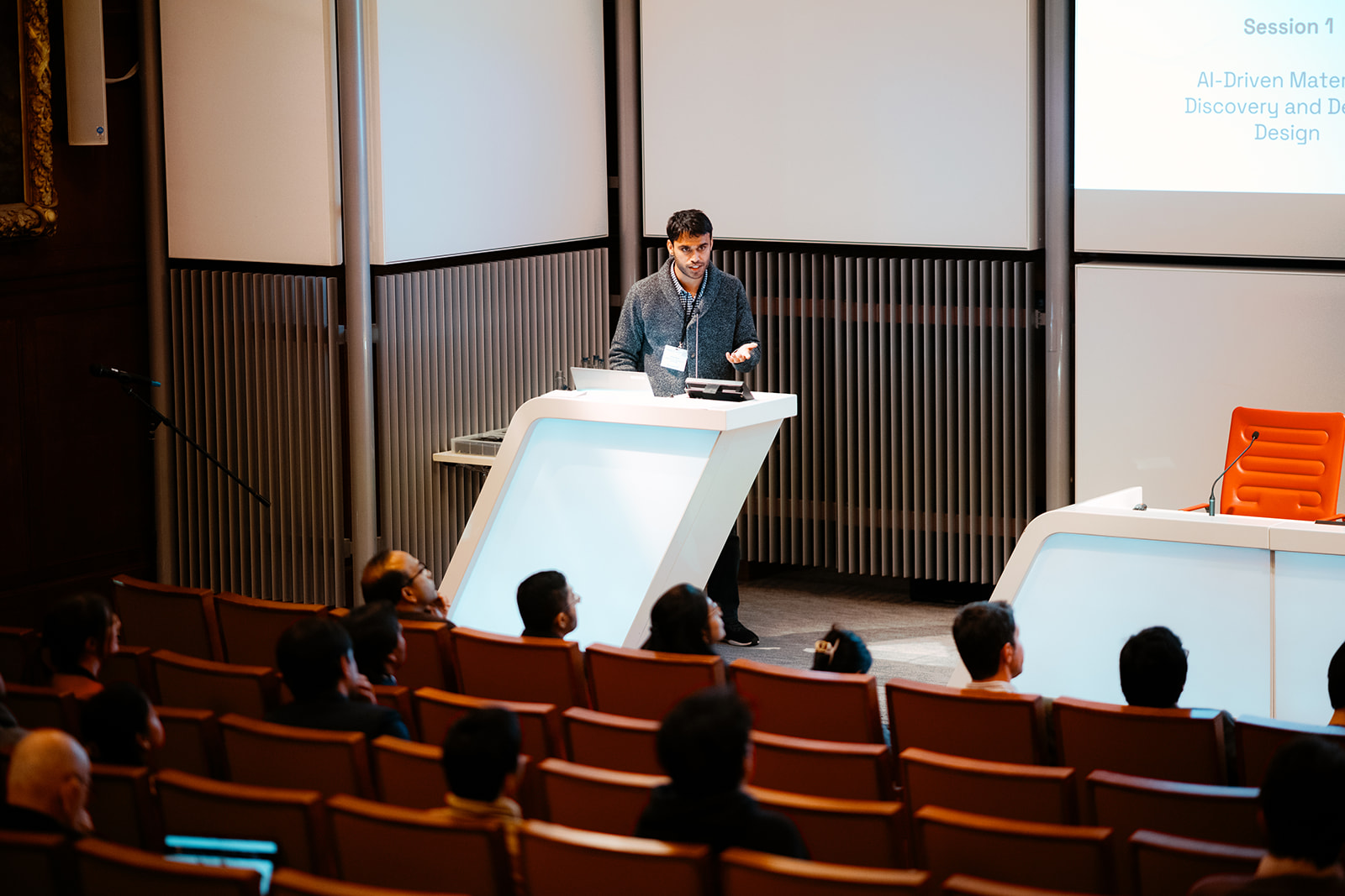
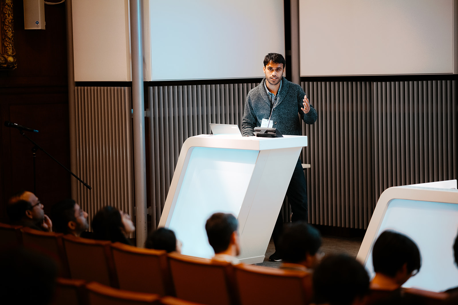
11:15 – 12:30 – AI-Driven Materials Discovery and Device Design
12:30 – 13:30 – Lunch
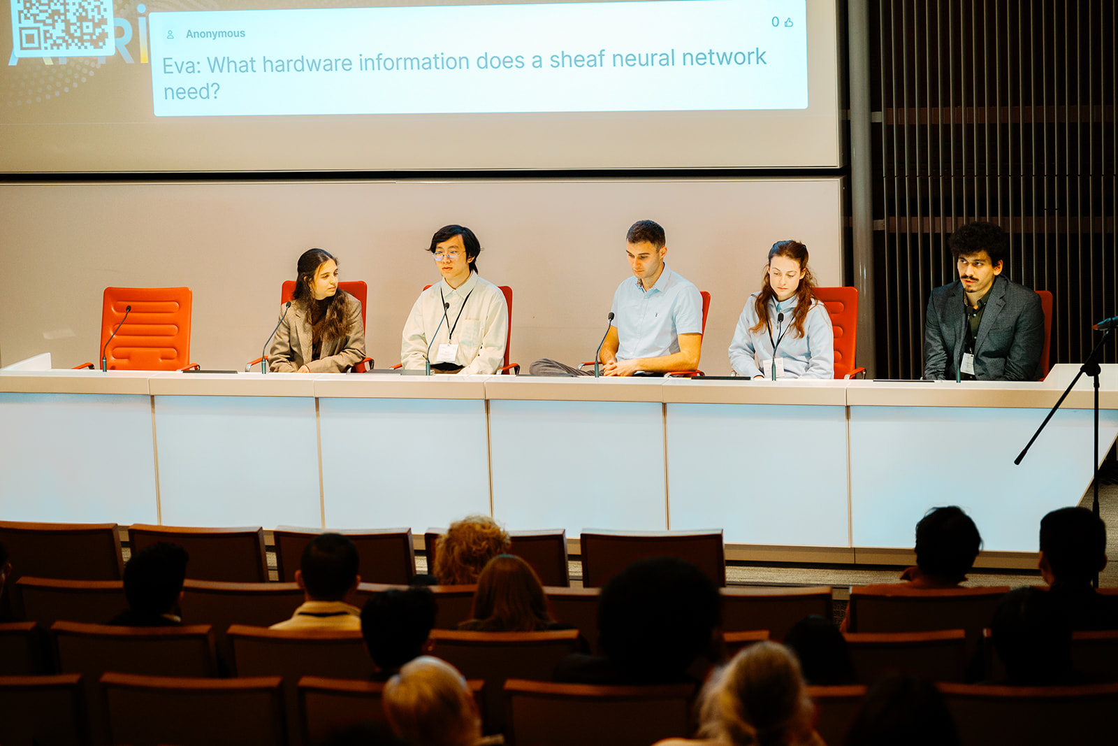
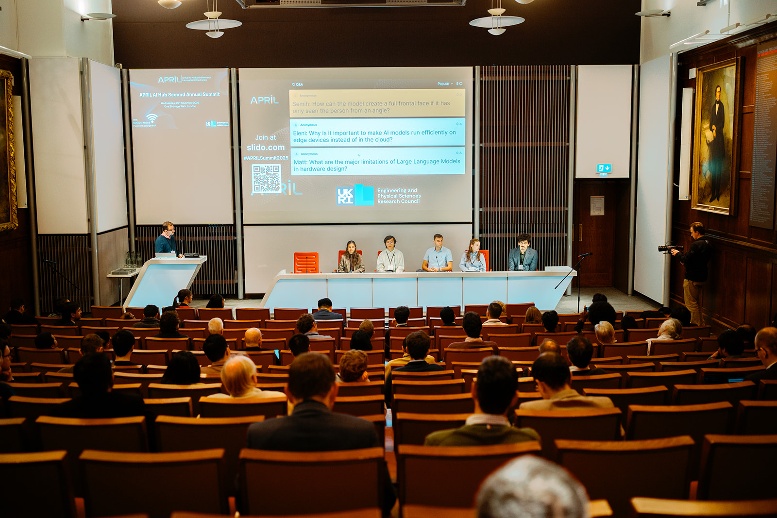
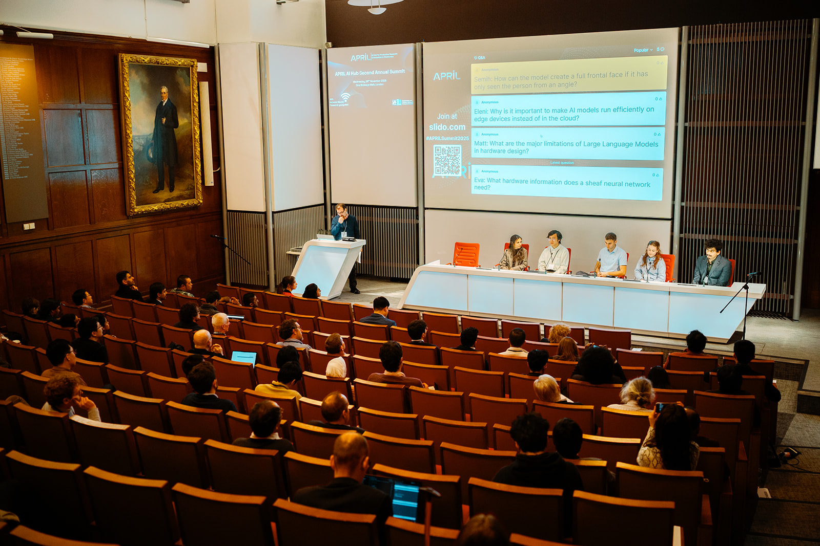
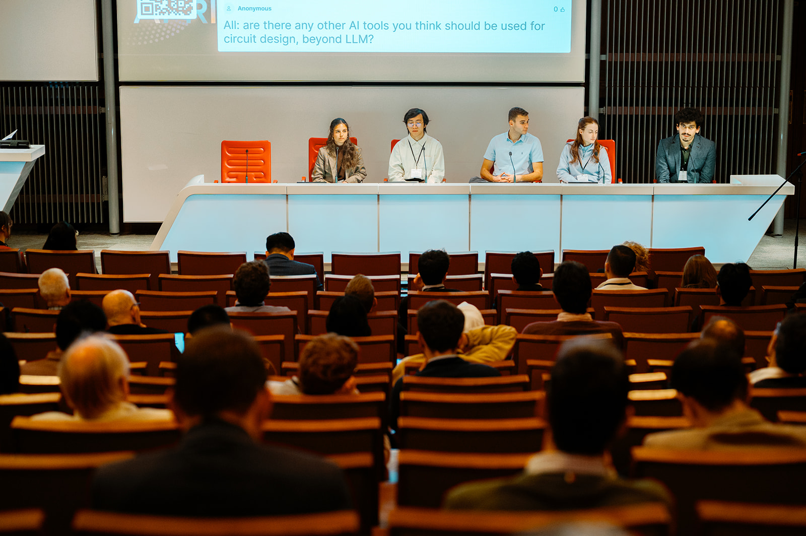
13:30 – 14:45 - AI-Driven Circuit Design and Verification Automation
14:45– 15:15– Afternoon Break
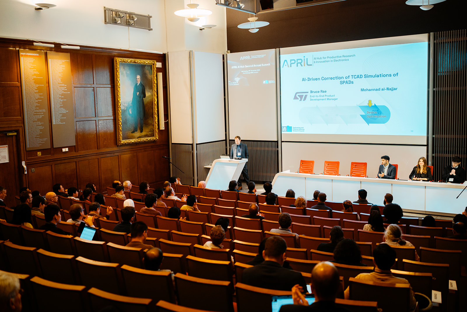
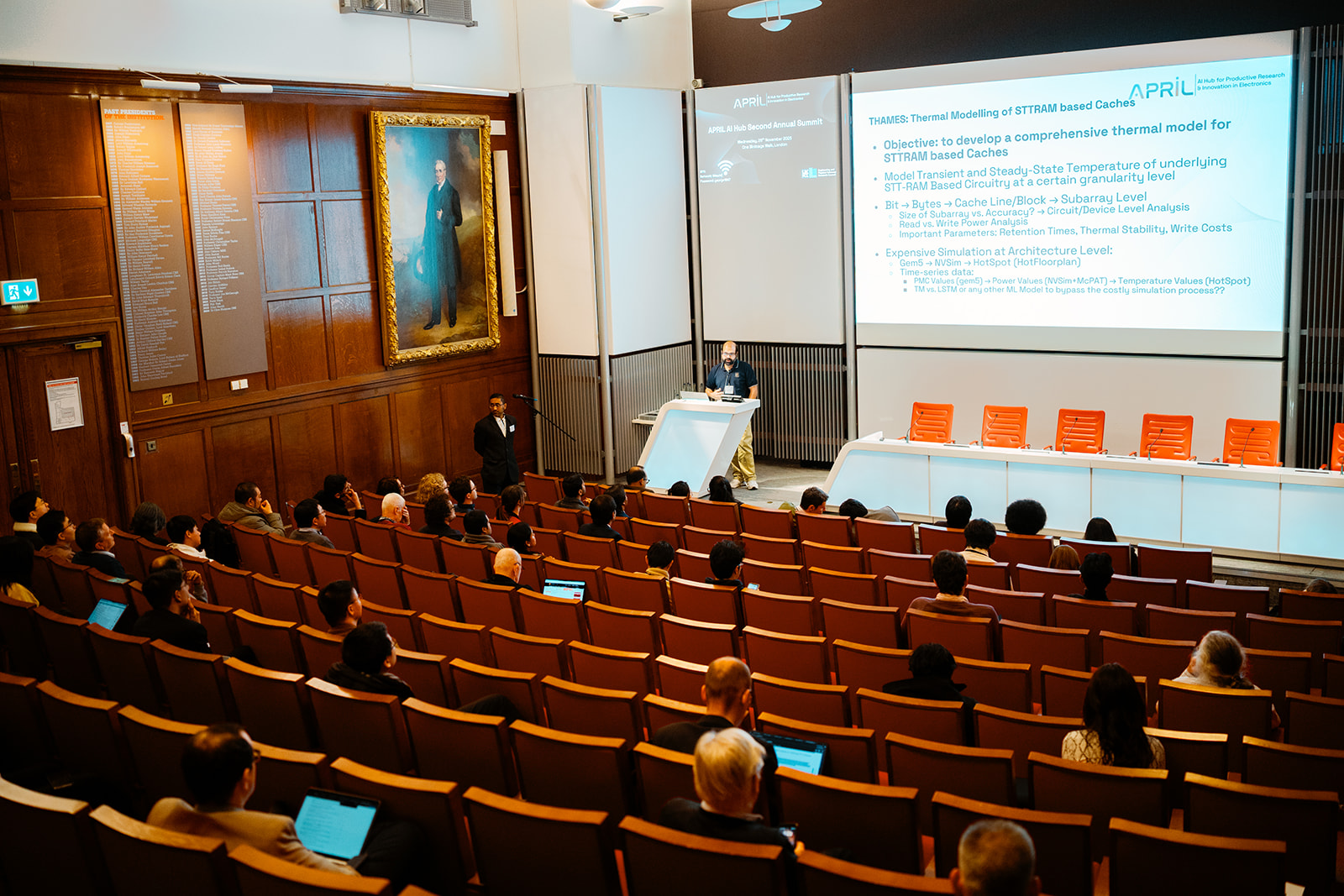
15:15 – 16:20 – Machine Learning for CMOS and Beyond CMOS Devices Design
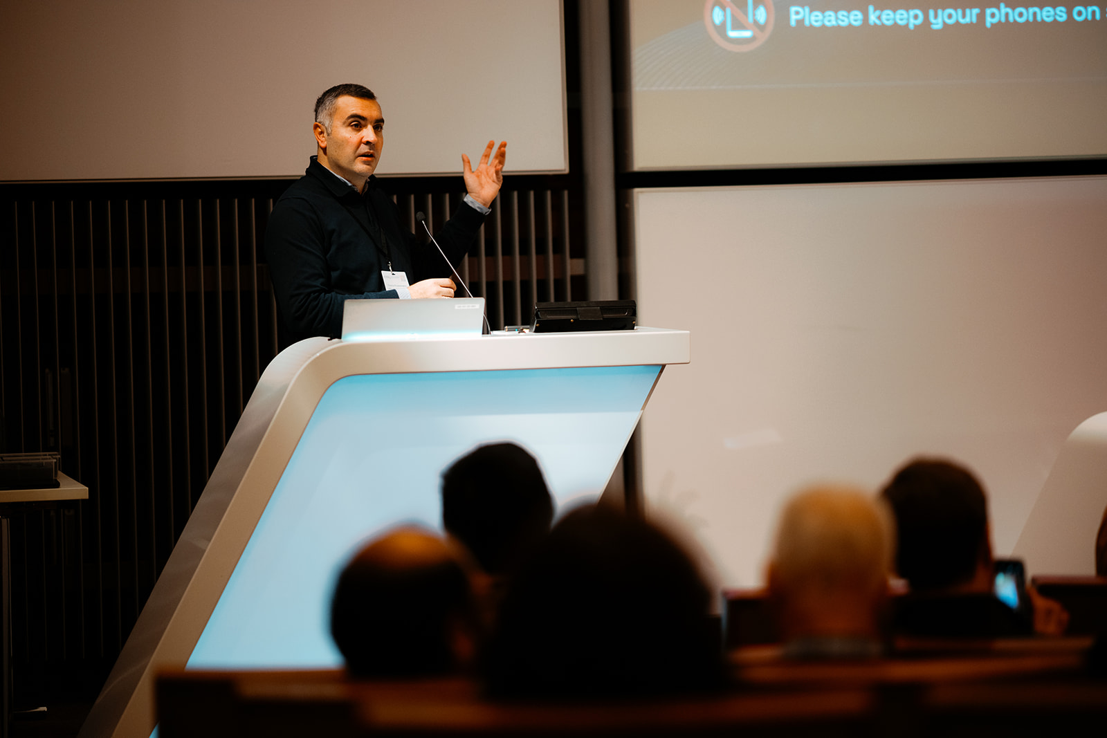
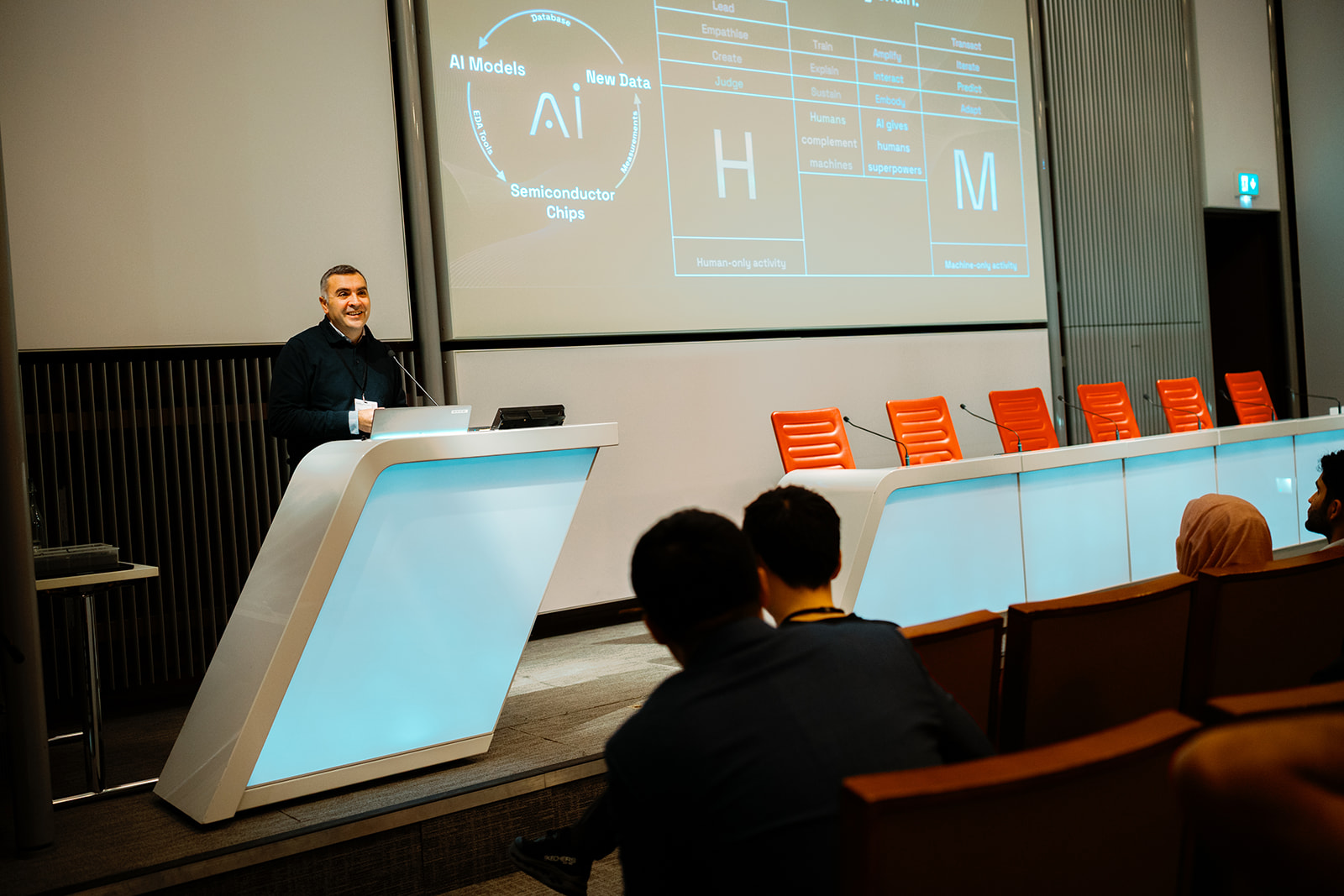
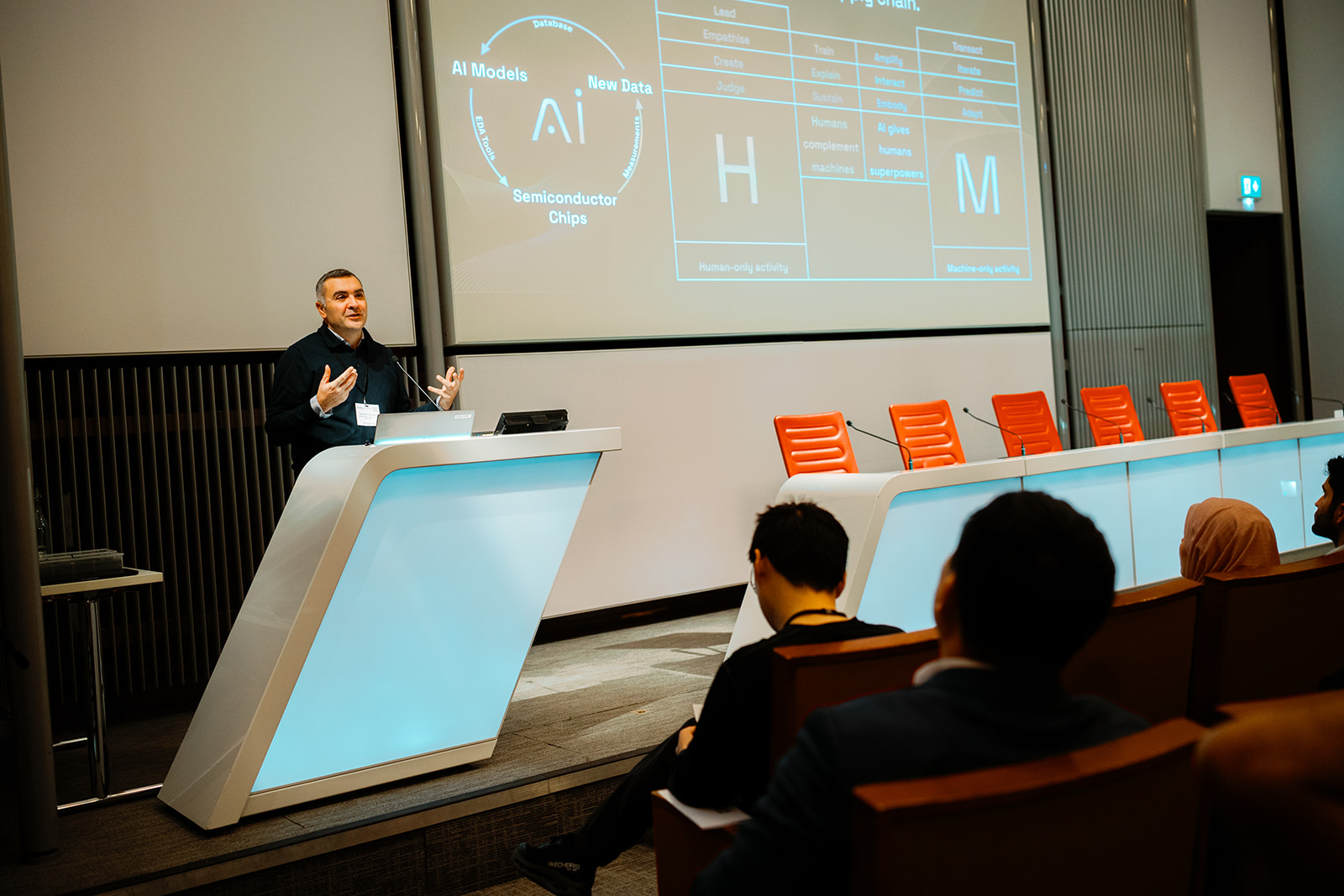
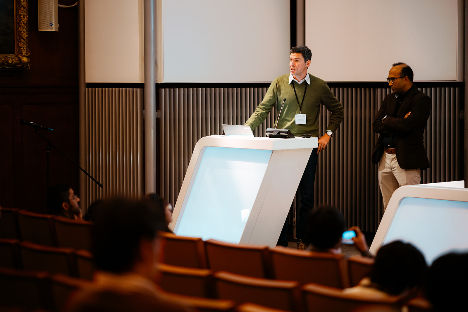
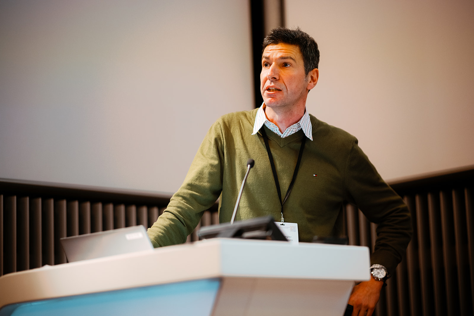
16:20 – 16:50 – The Through Line of AI for Electronics
16:50 – 17:00 – Closing Remarks
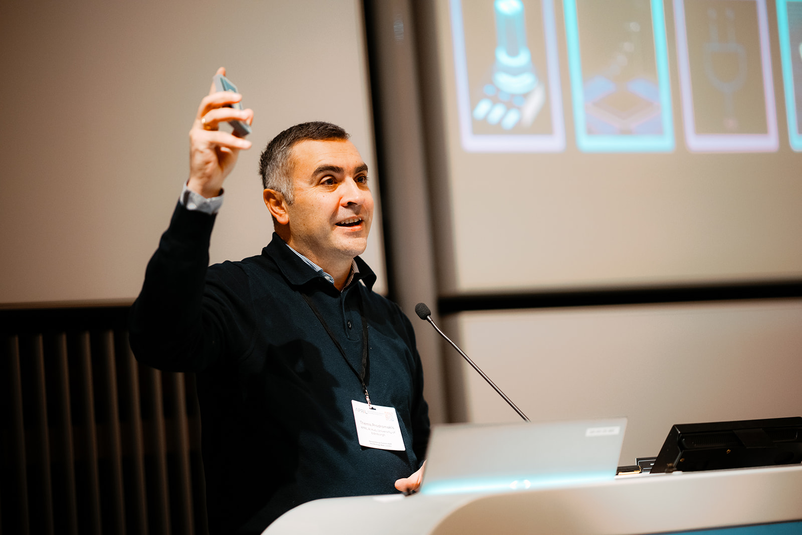
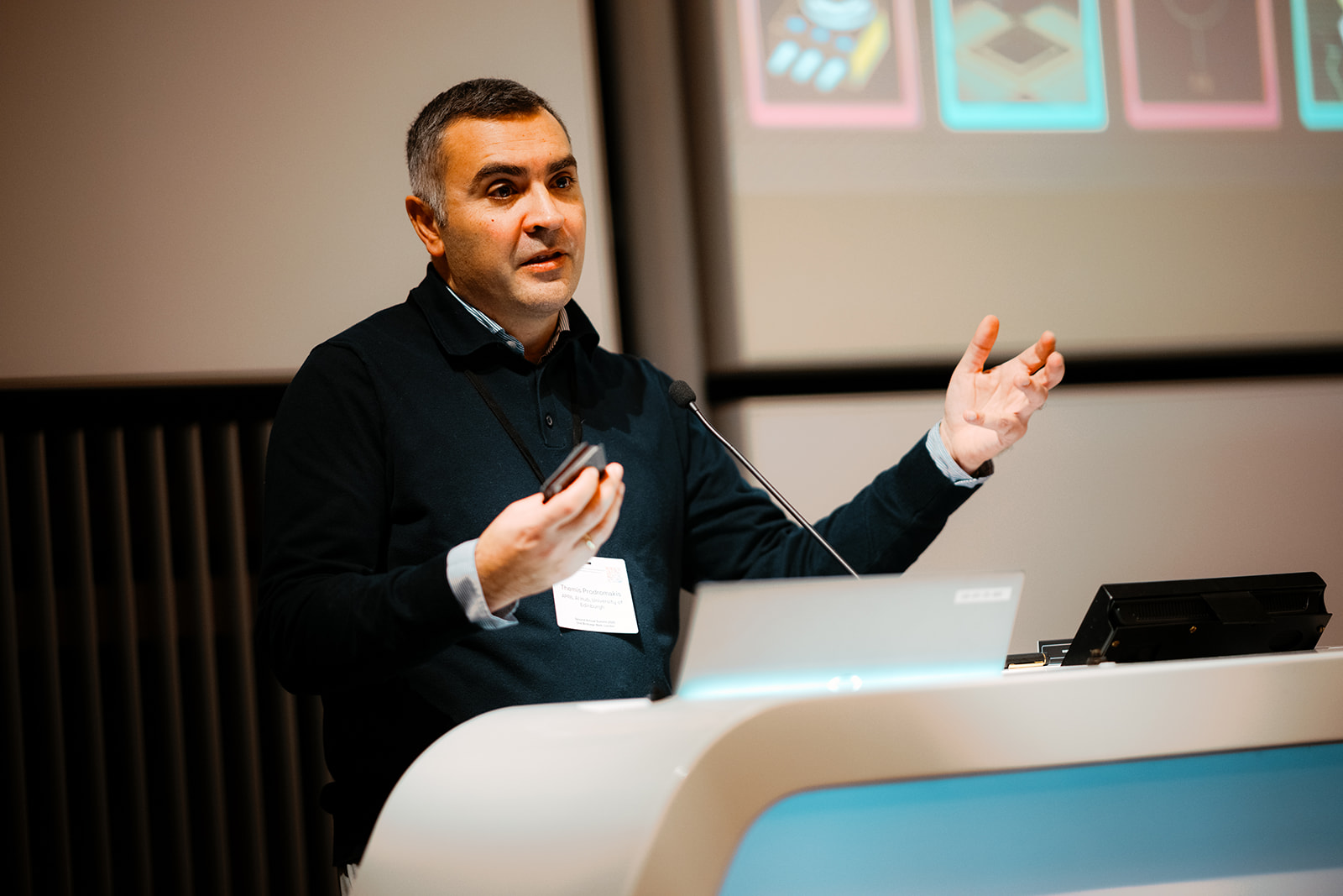
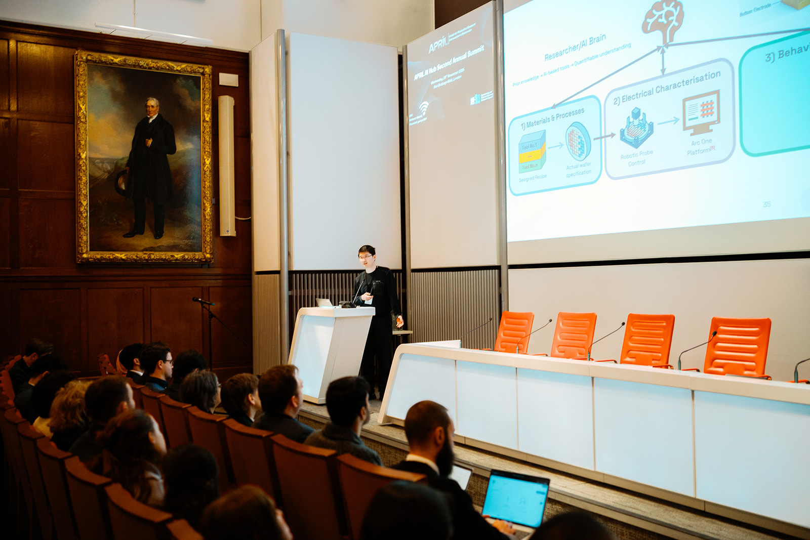
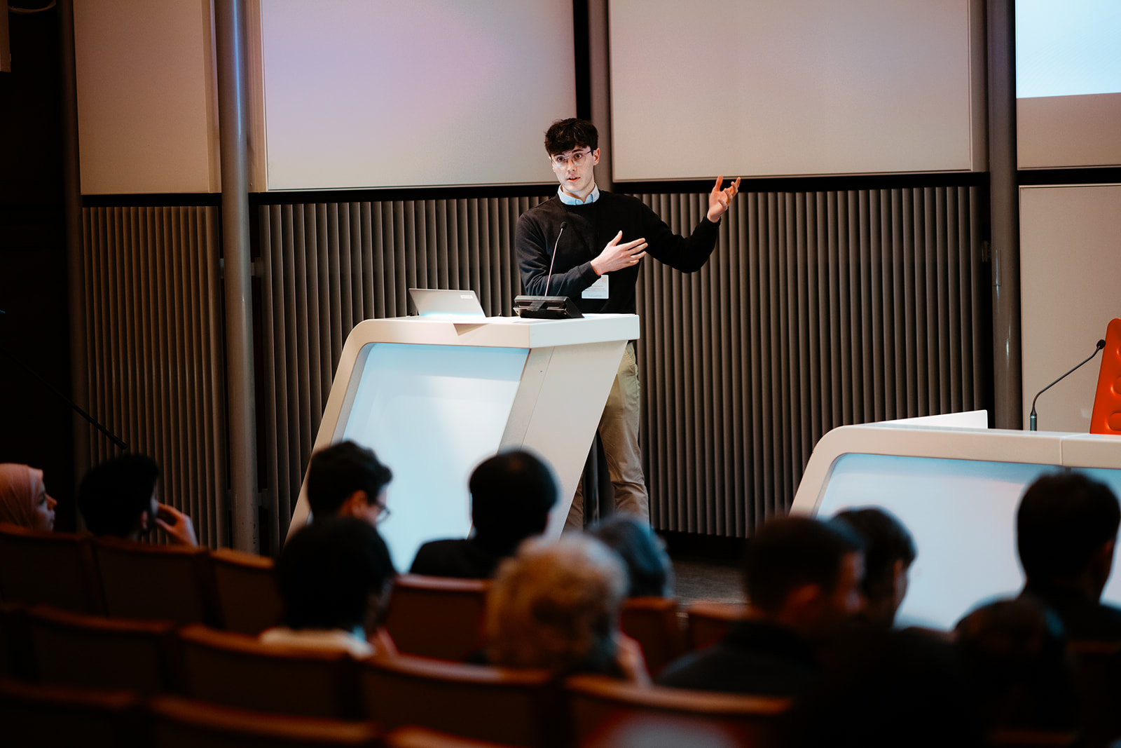
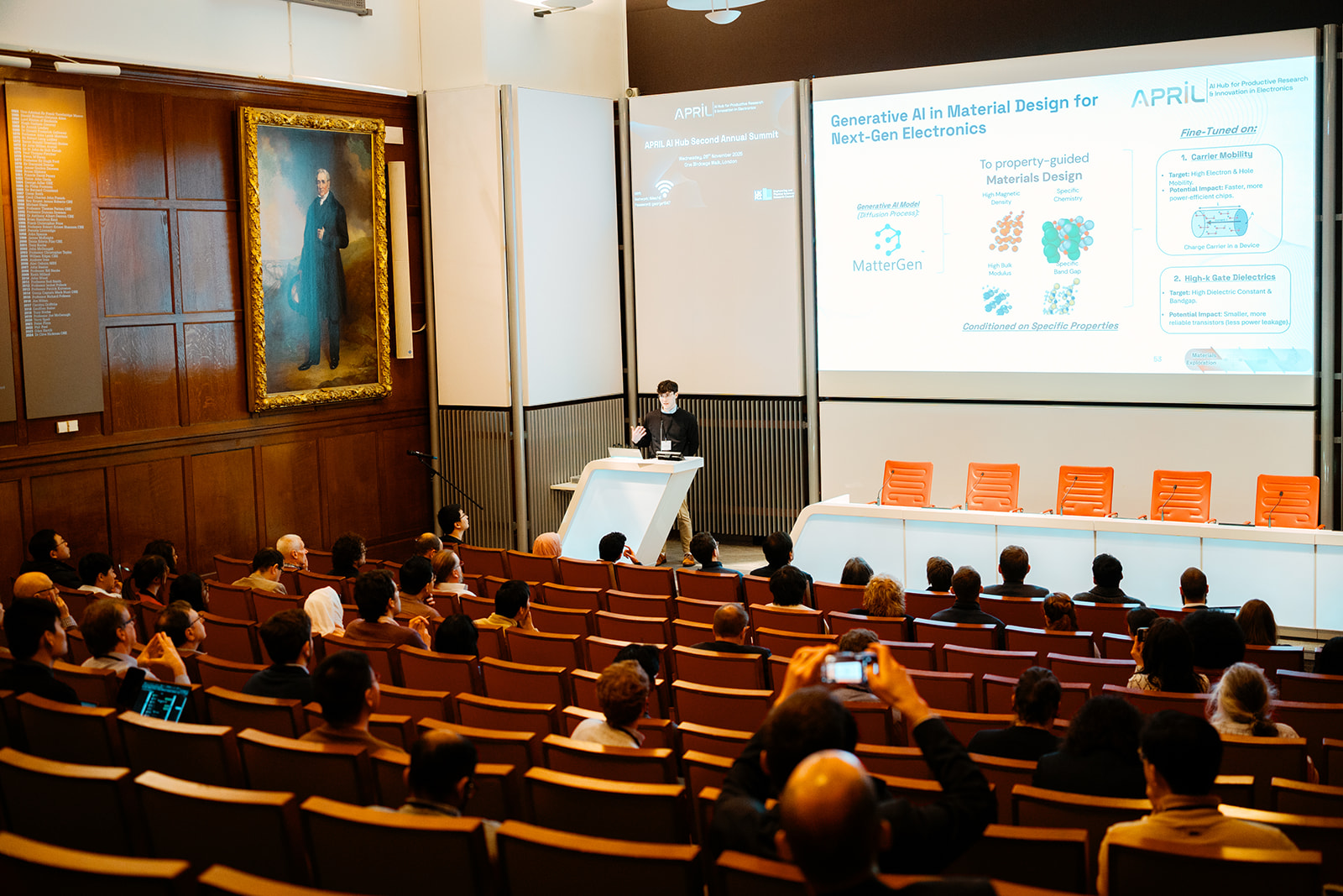
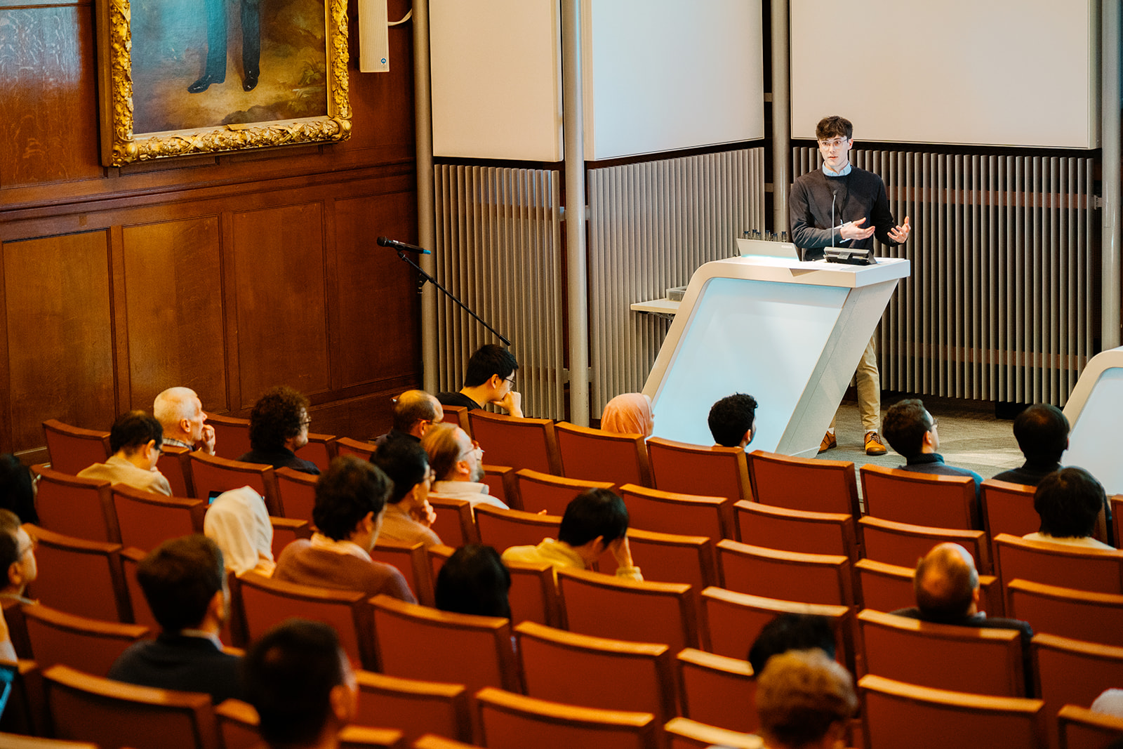
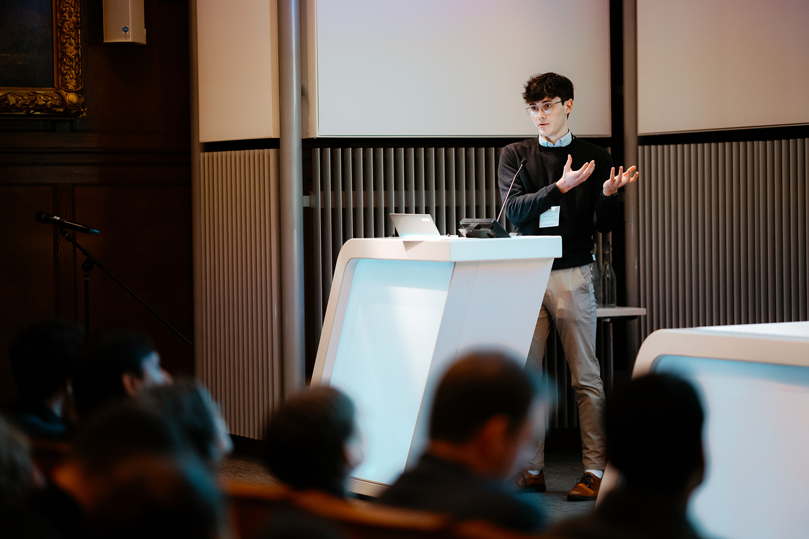
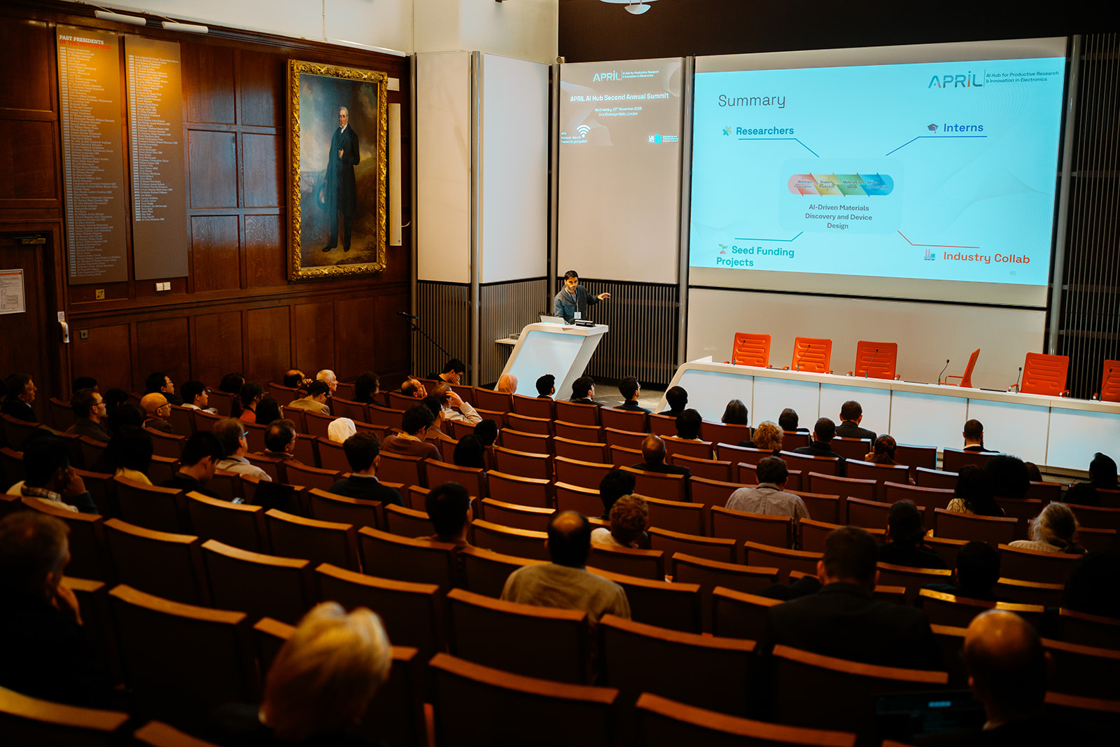
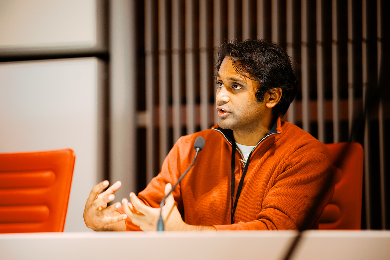
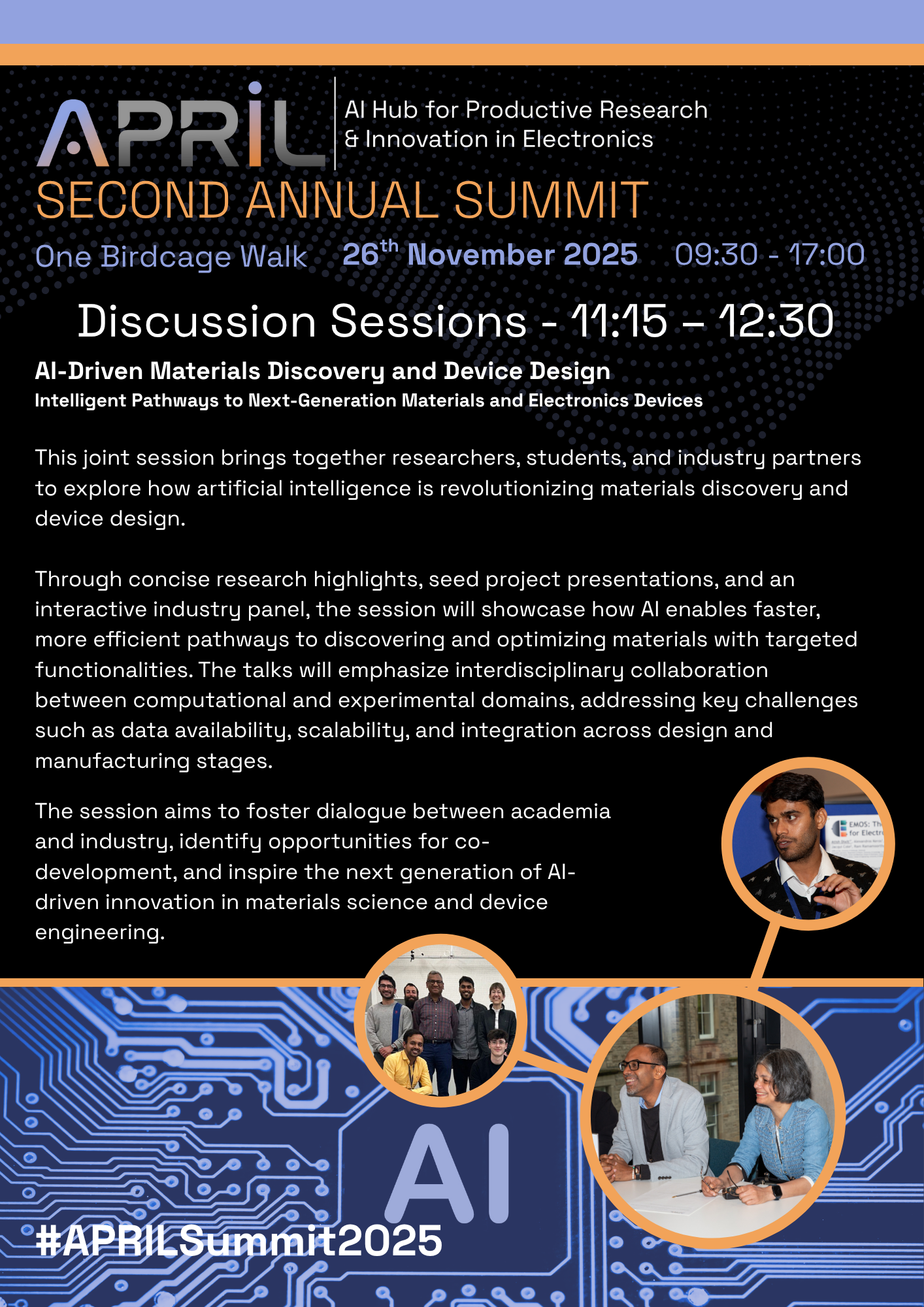
AI-Driven Materials Discovery and Device Design - 11:15 – 12:30
Intelligent Pathways to Next-Generation Materials and Electronics Devices
This joint session brings together researchers, students, and industry partners to explore how artificial intelligence is revolutionizing materials discovery and device design.
Through concise research highlights and seed project presentations, the session will showcase how AI enables faster, more efficient pathways to discovering and optimizing materials with targeted functionalities. The talks will emphasize interdisciplinary collaboration between computational and experimental domains, addressing key challenges such as data availability, scalability, and integration across design and manufacturing stages.
The session aims to foster dialogue between academia and industry, identify opportunities for co-development, and inspire the next generation of AI-driven innovation in materials science and device engineering.
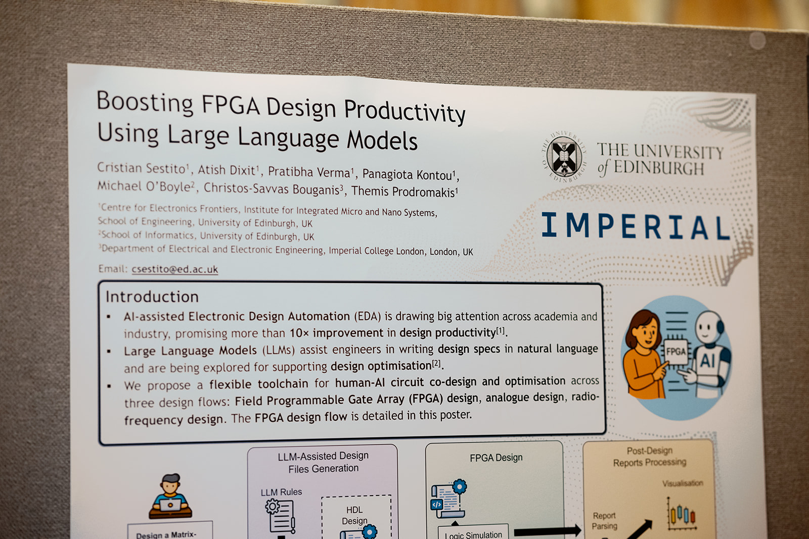
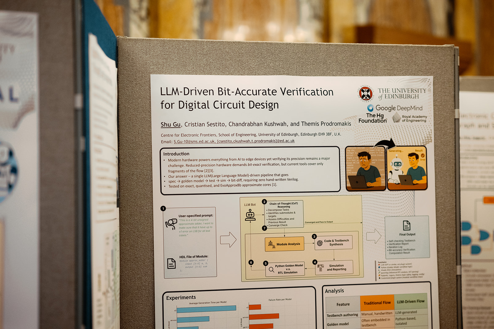
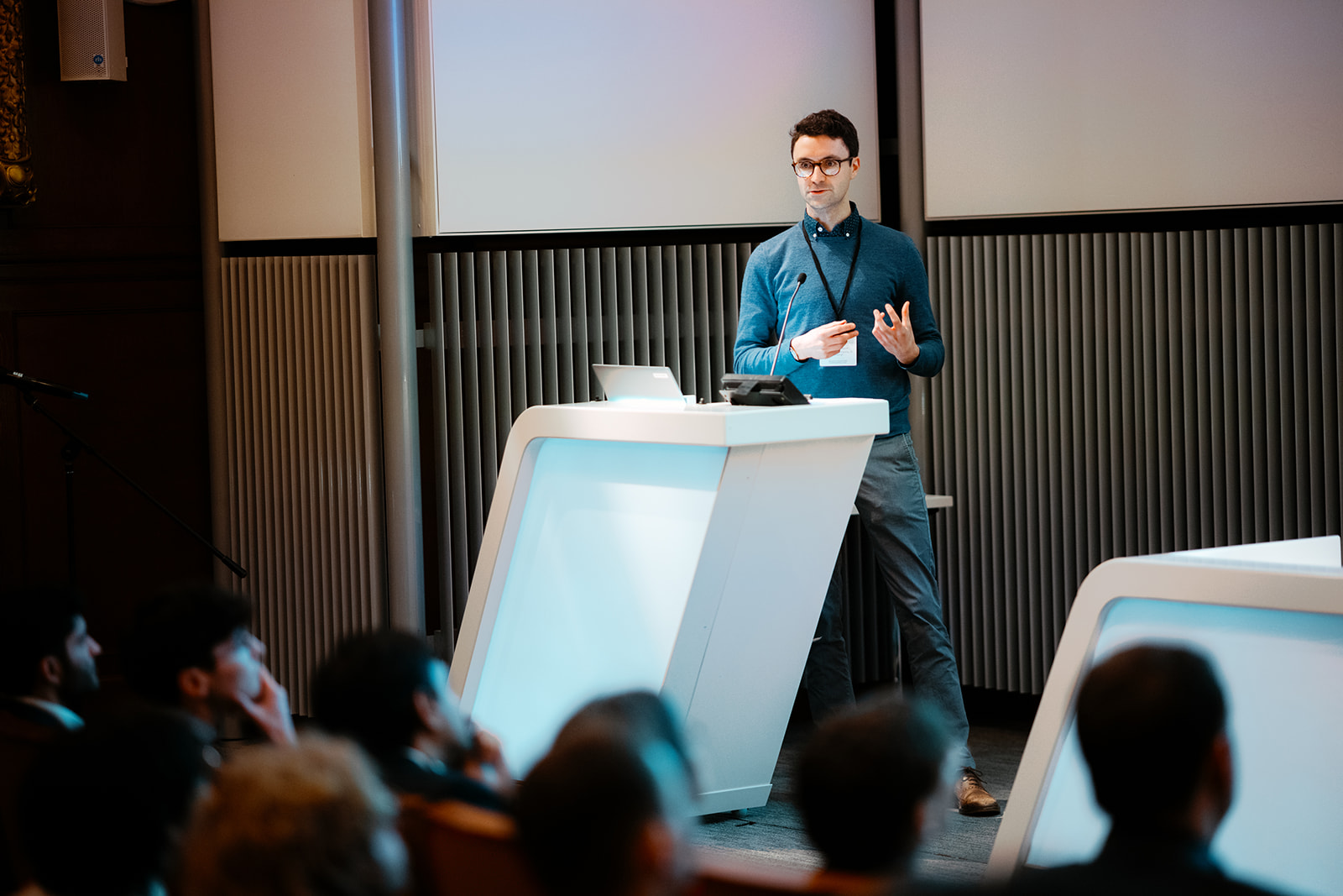
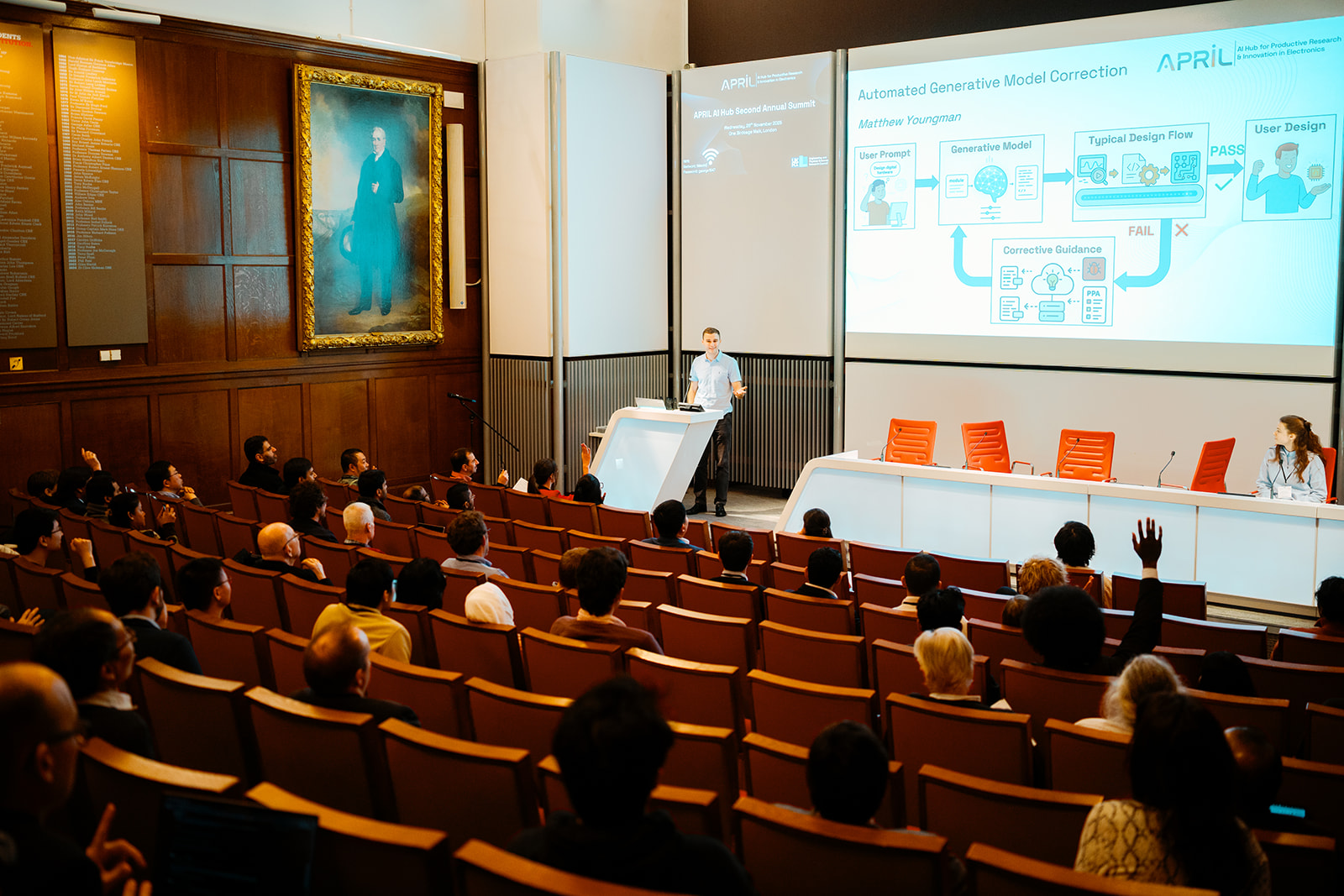
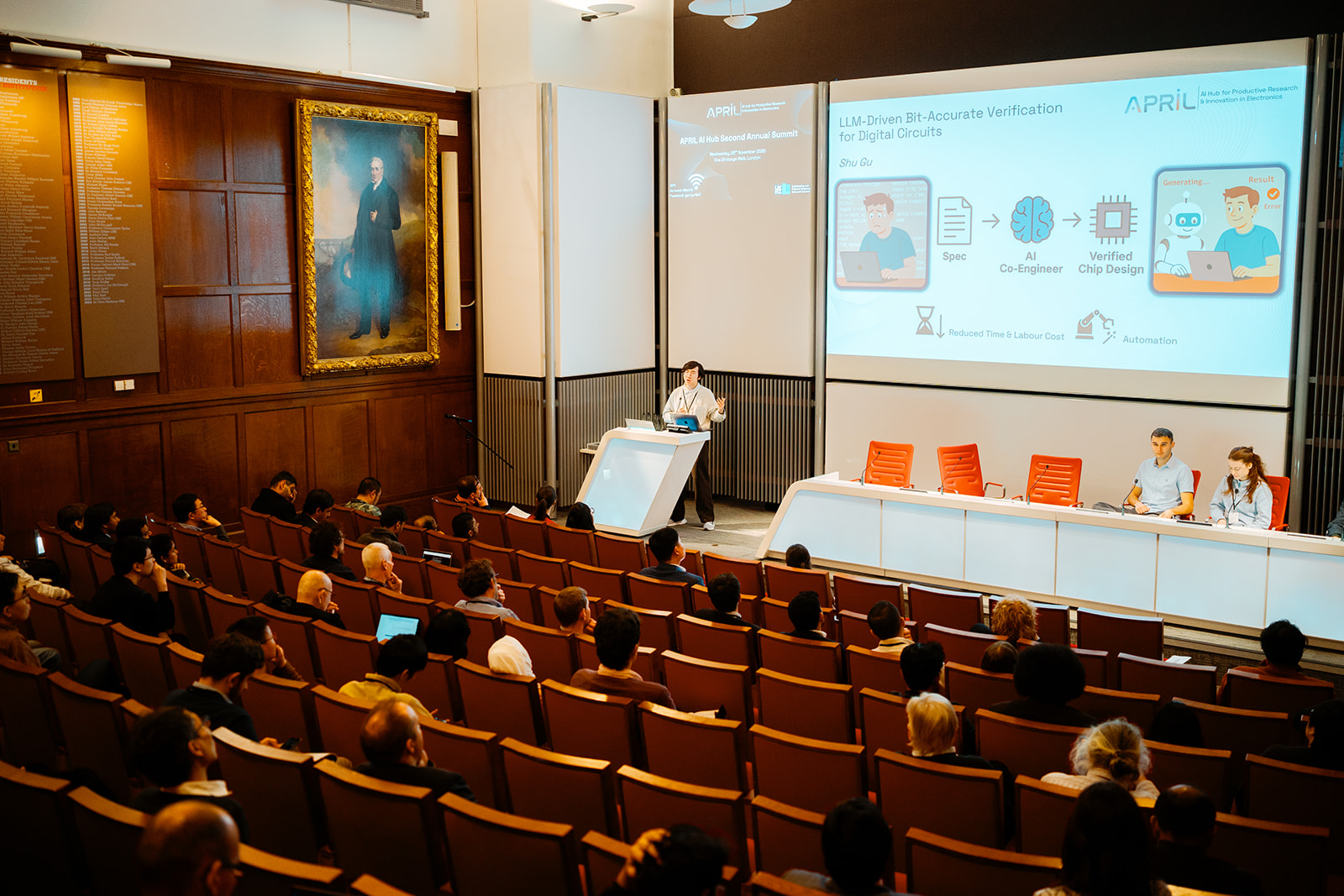
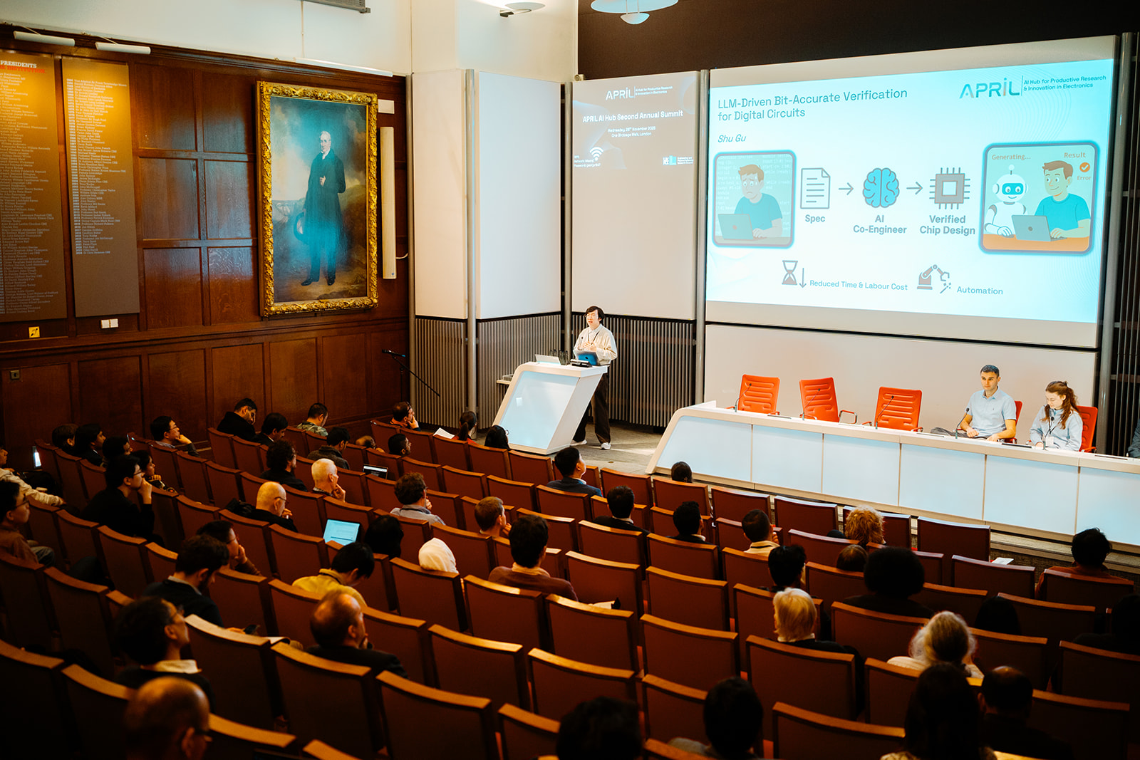
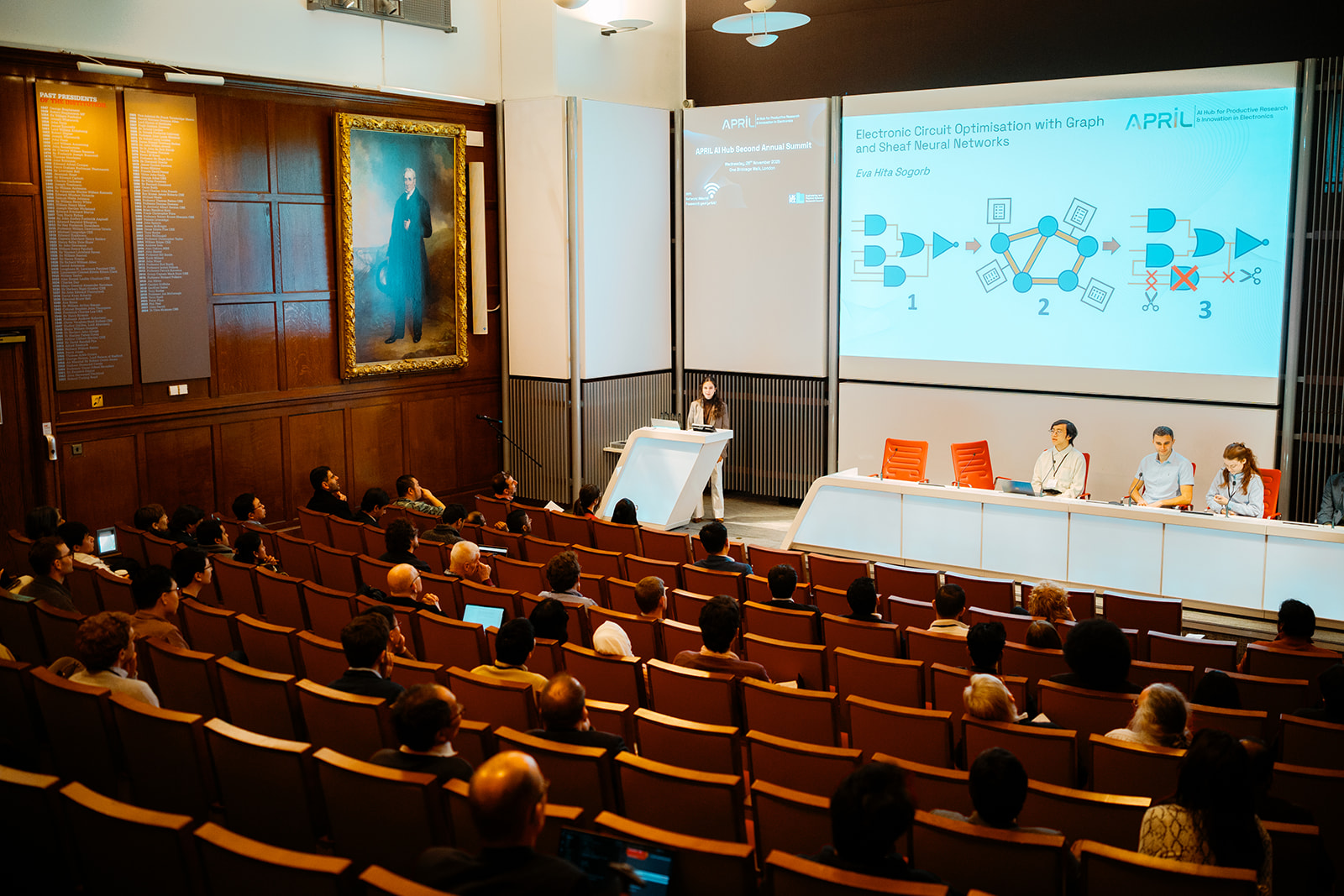
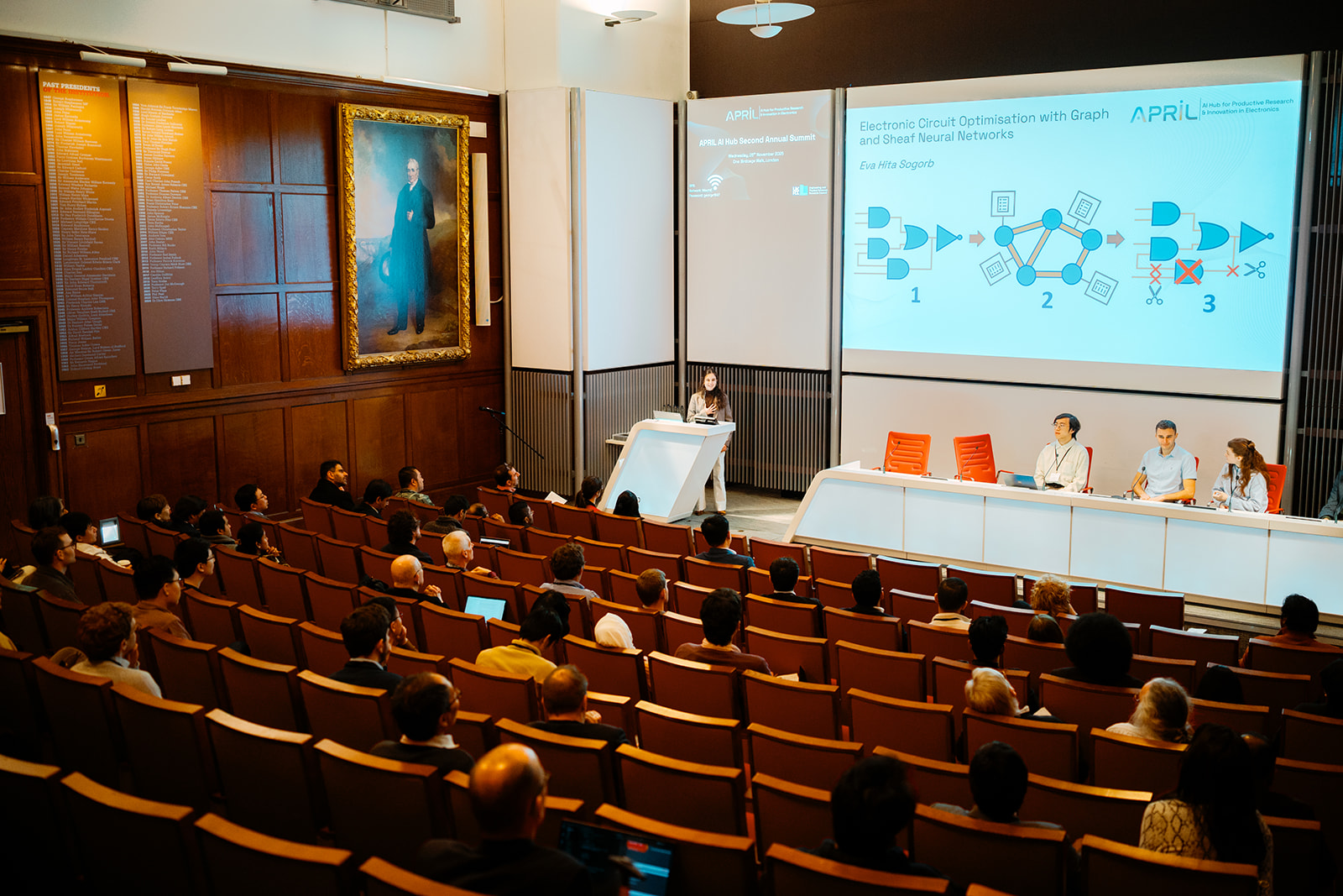
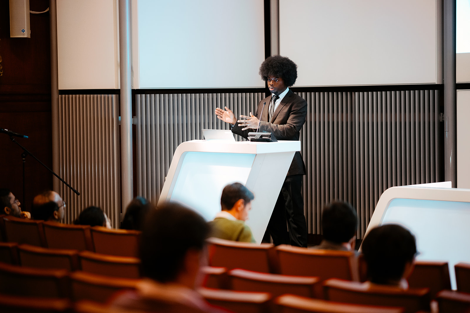
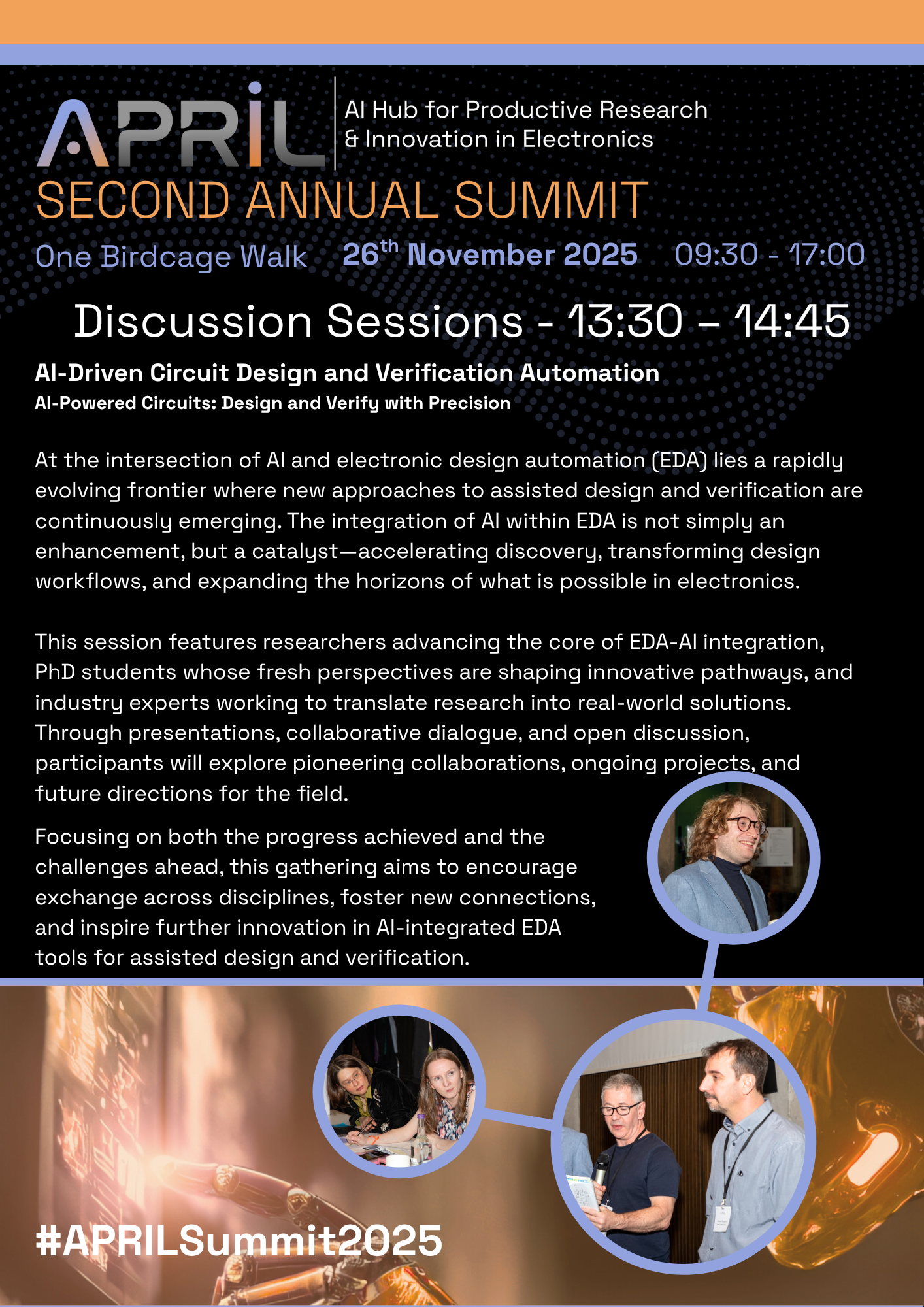
AI-Driven Circuit Design and Verification Automation - 13:30 – 14:45
AI-Powered Circuits: Design and Verify with Precision
At the intersection of AI and electronic design automation (EDA) lies a rapidly evolving frontier where new approaches to assisted design and verification are continuously emerging. The integration of AI within EDA is not simply an enhancement, but a catalyst—accelerating discovery, transforming design workflows, and expanding the horizons of what is possible in electronics.
This session features researchers advancing the core of EDA-AI integration, PhD students whose fresh perspectives are shaping innovative pathways, and industry experts working to translate research into real-world solutions. Through presentations, collaborative dialogue, and open discussion, participants will explore pioneering collaborations, ongoing projects, and future directions for the field.
Focusing on both the progress achieved and the challenges ahead, this gathering aims to encourage exchange across disciplines, foster new connections, and inspire further innovation in AI-integrated EDA tools for assisted design and verification.
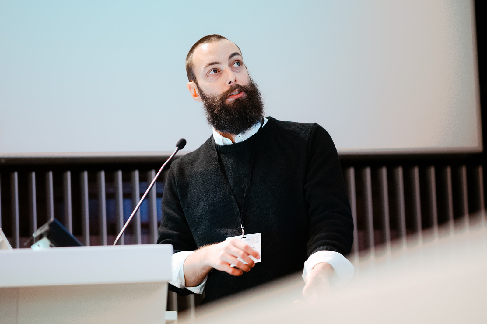
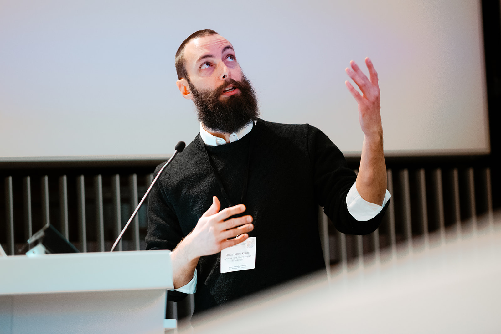
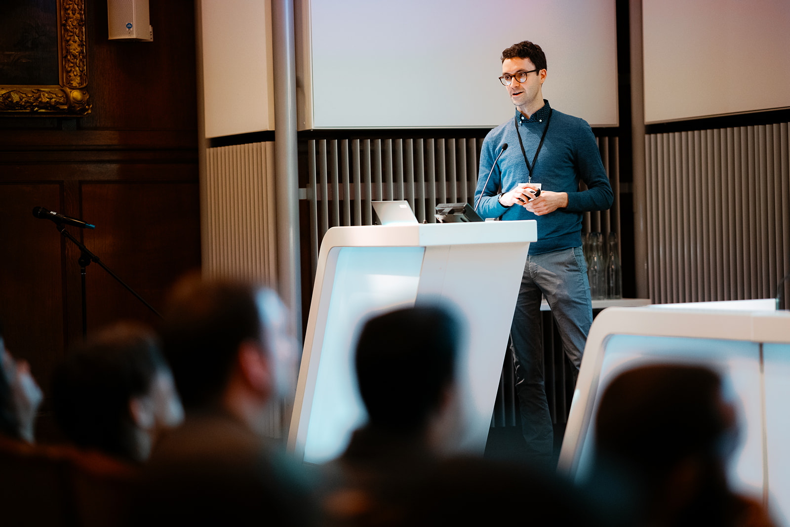
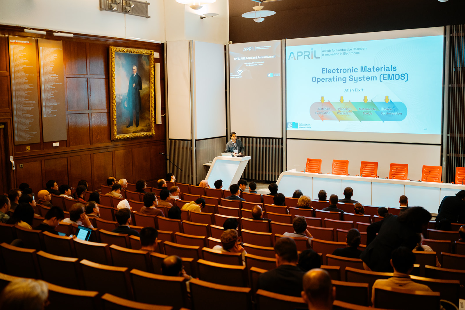
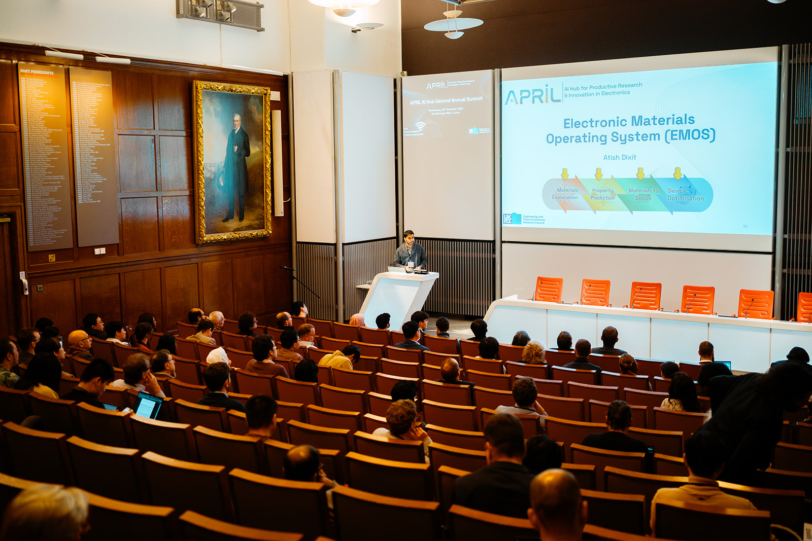
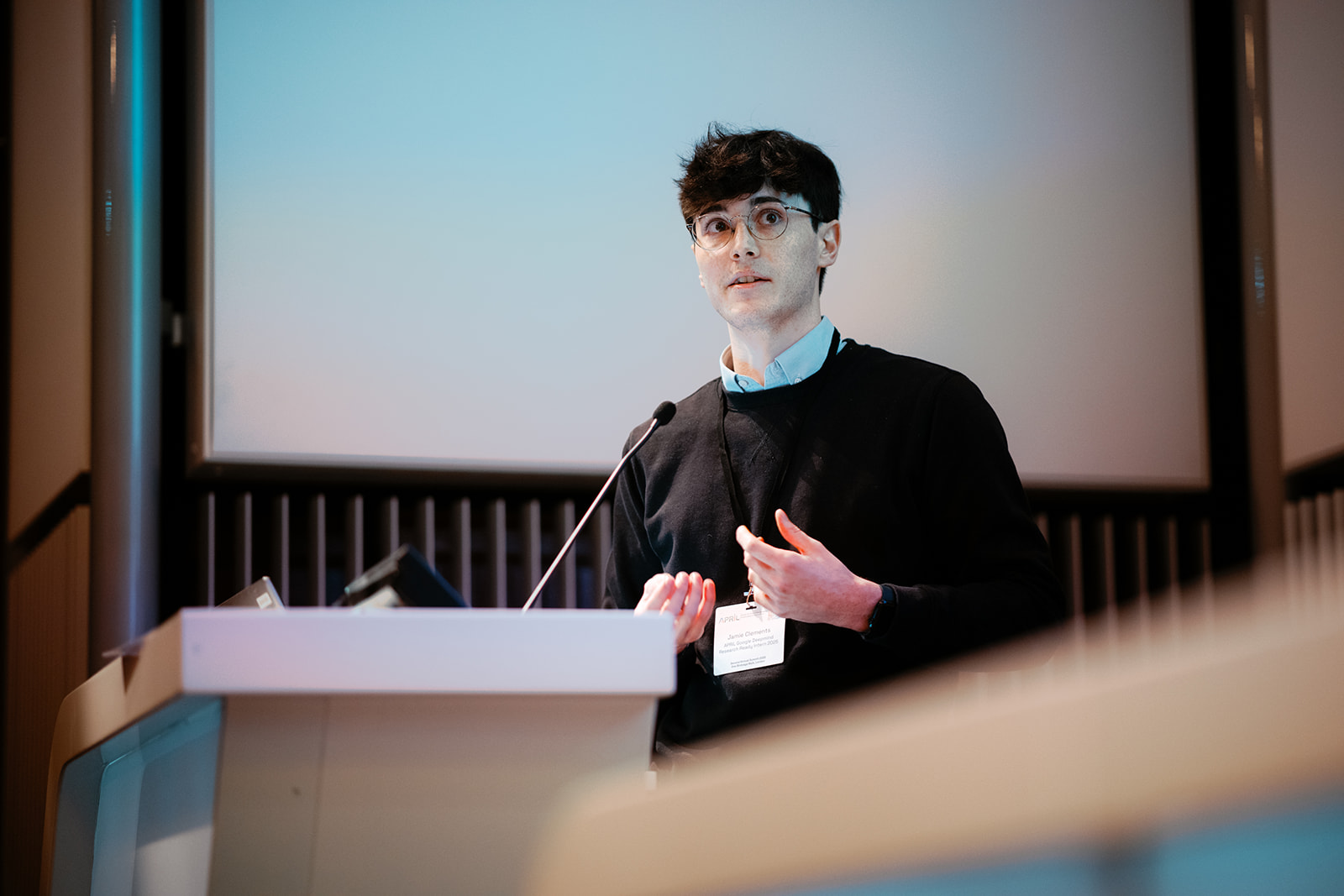
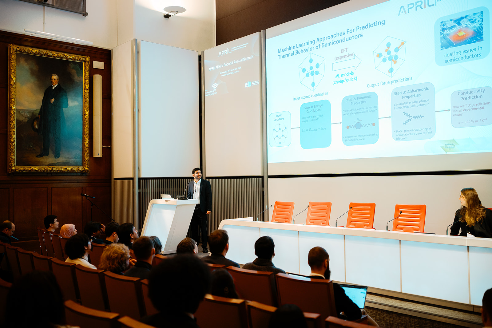
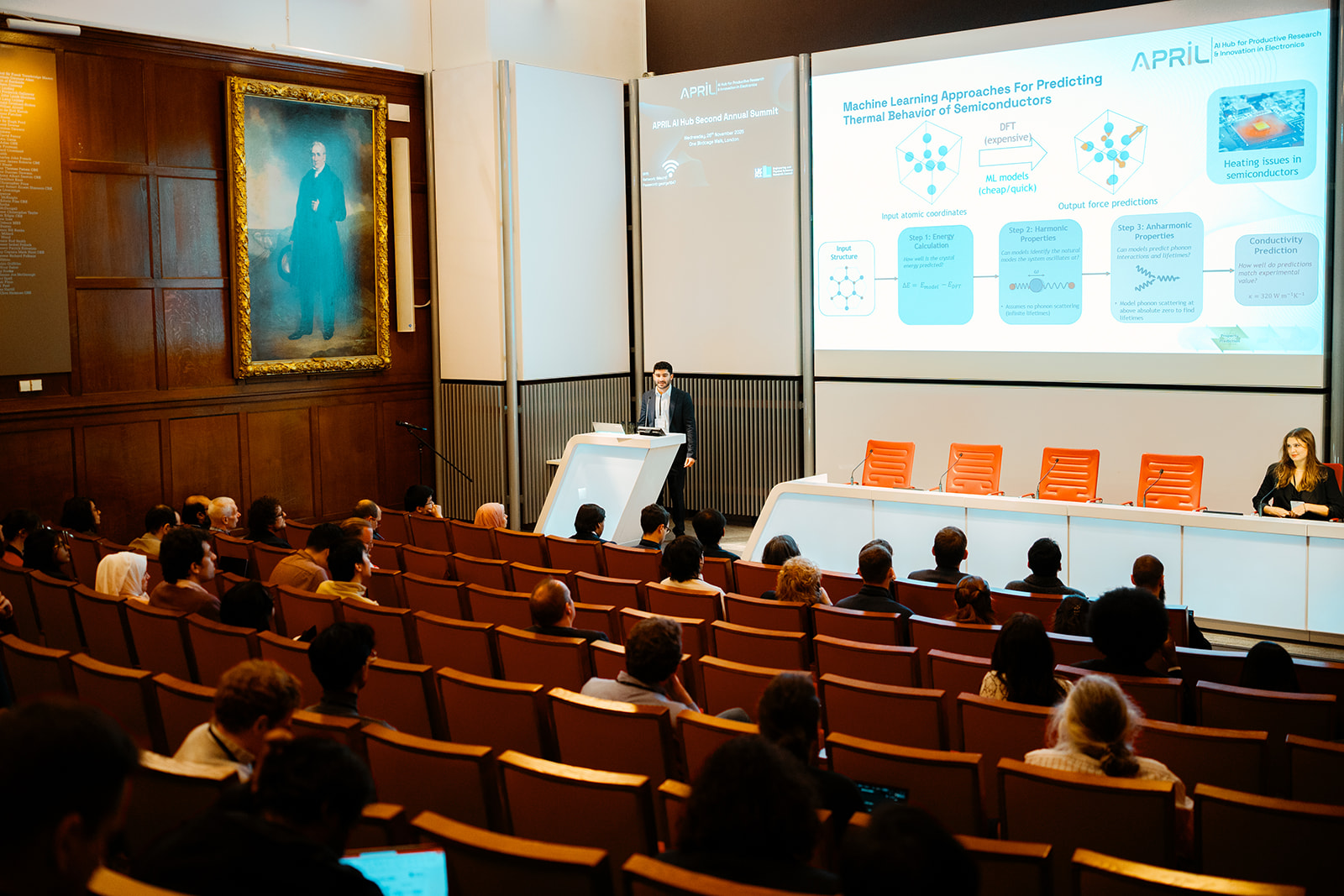
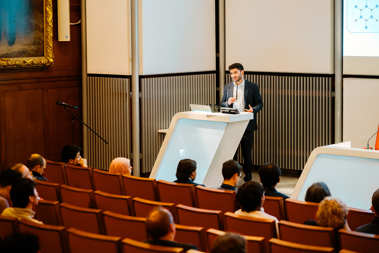
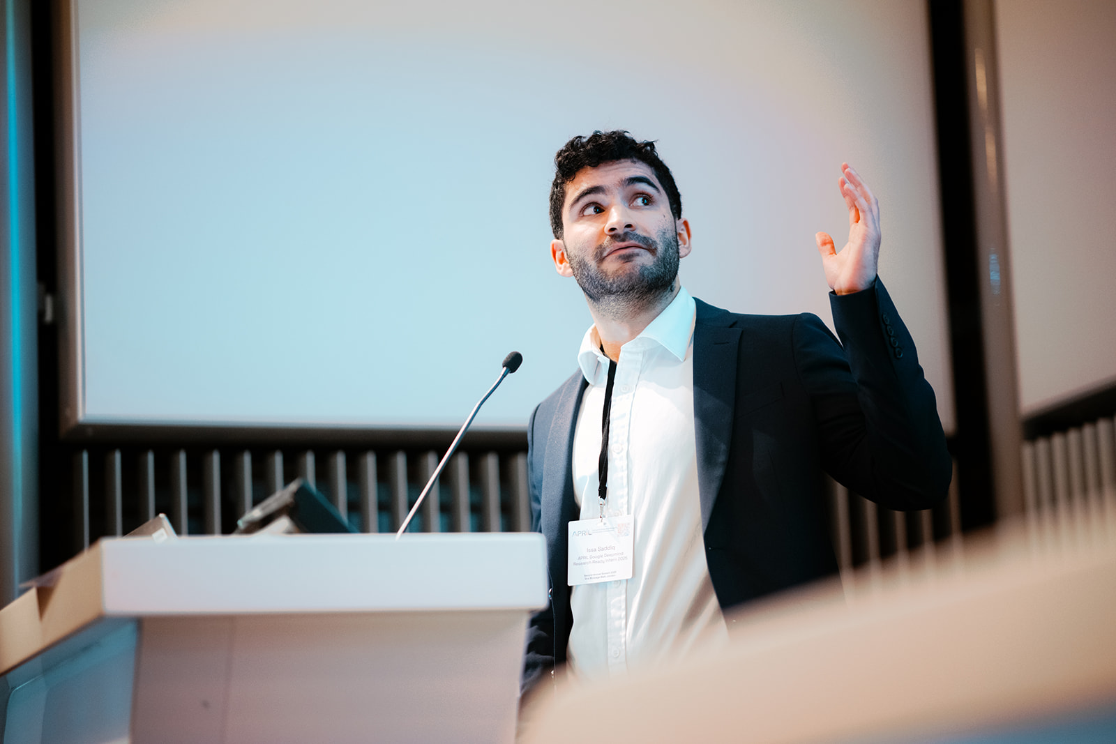
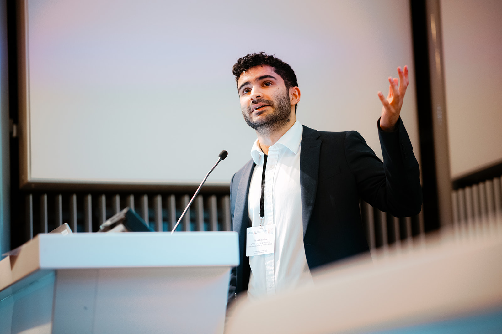
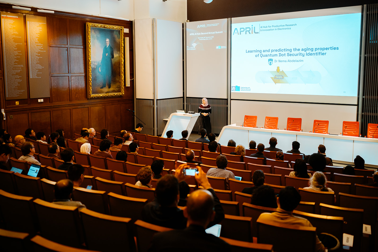
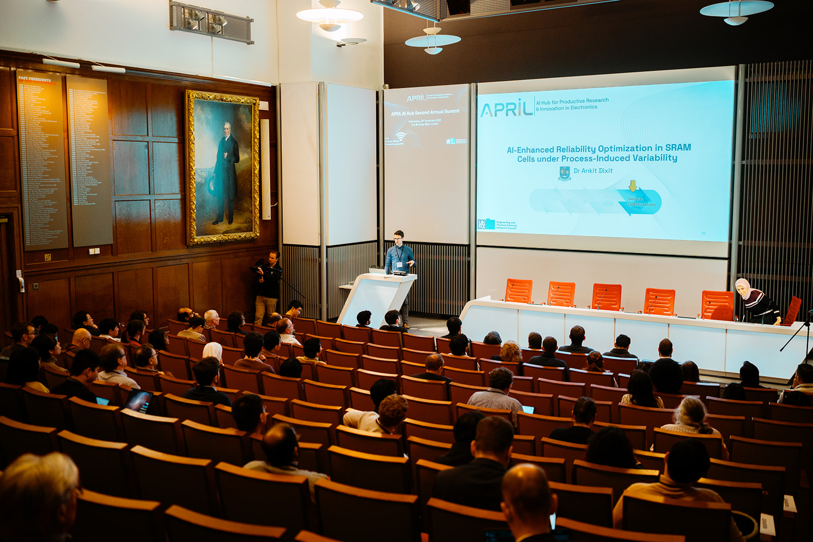
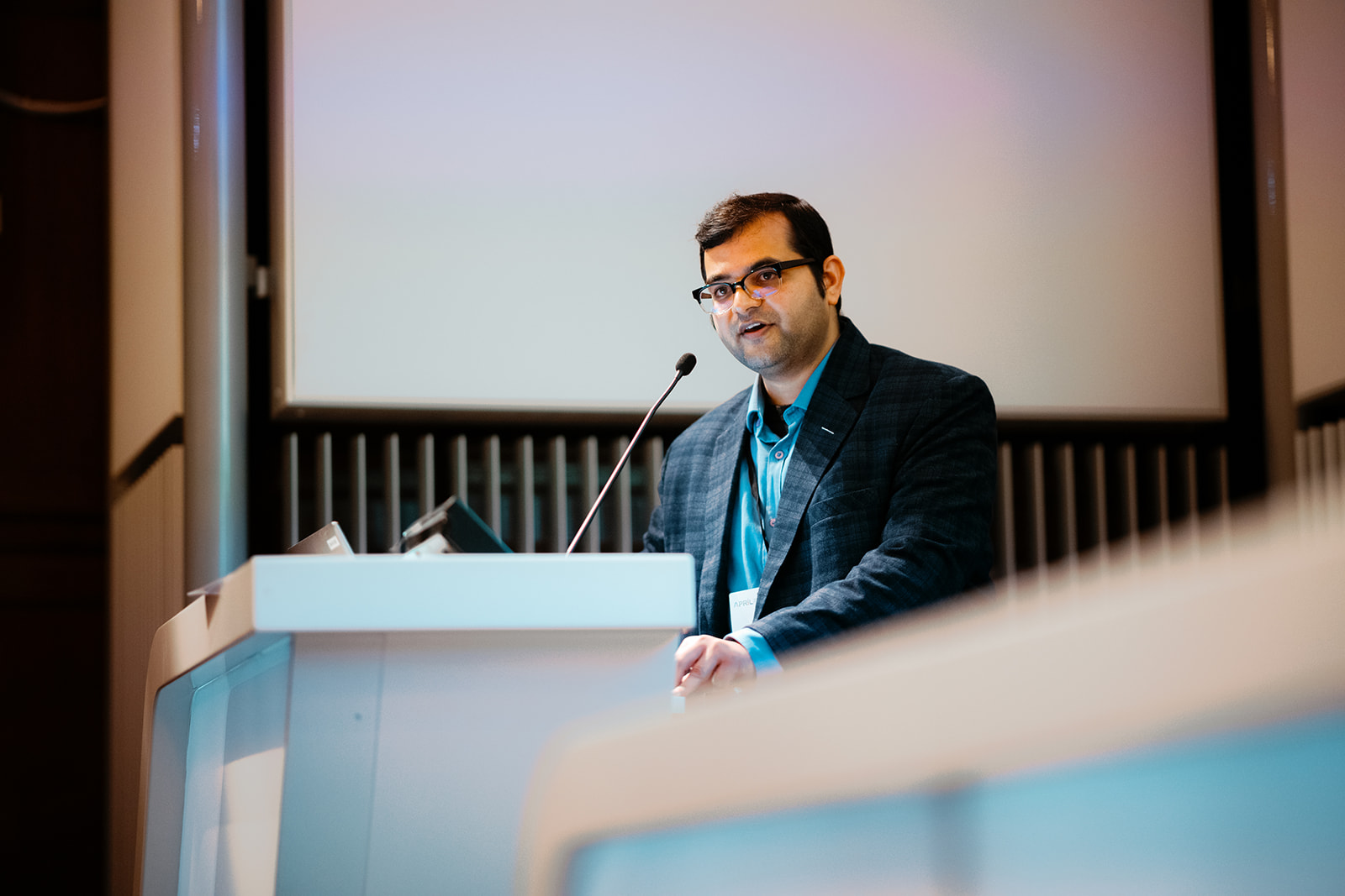
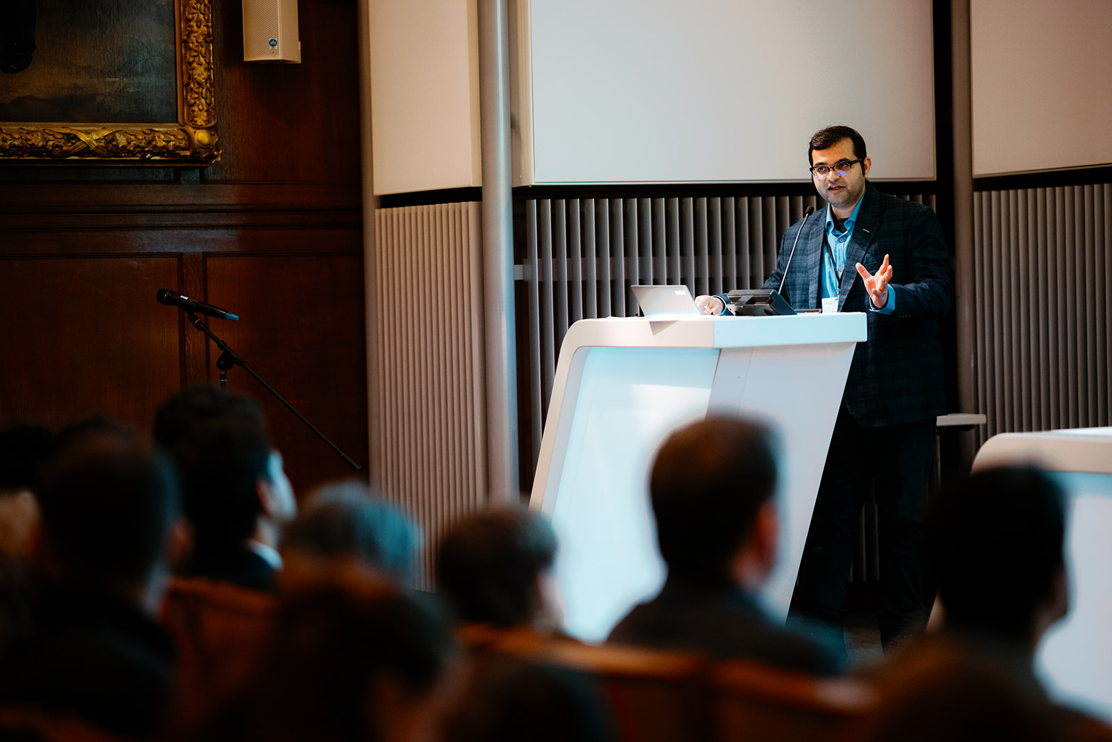
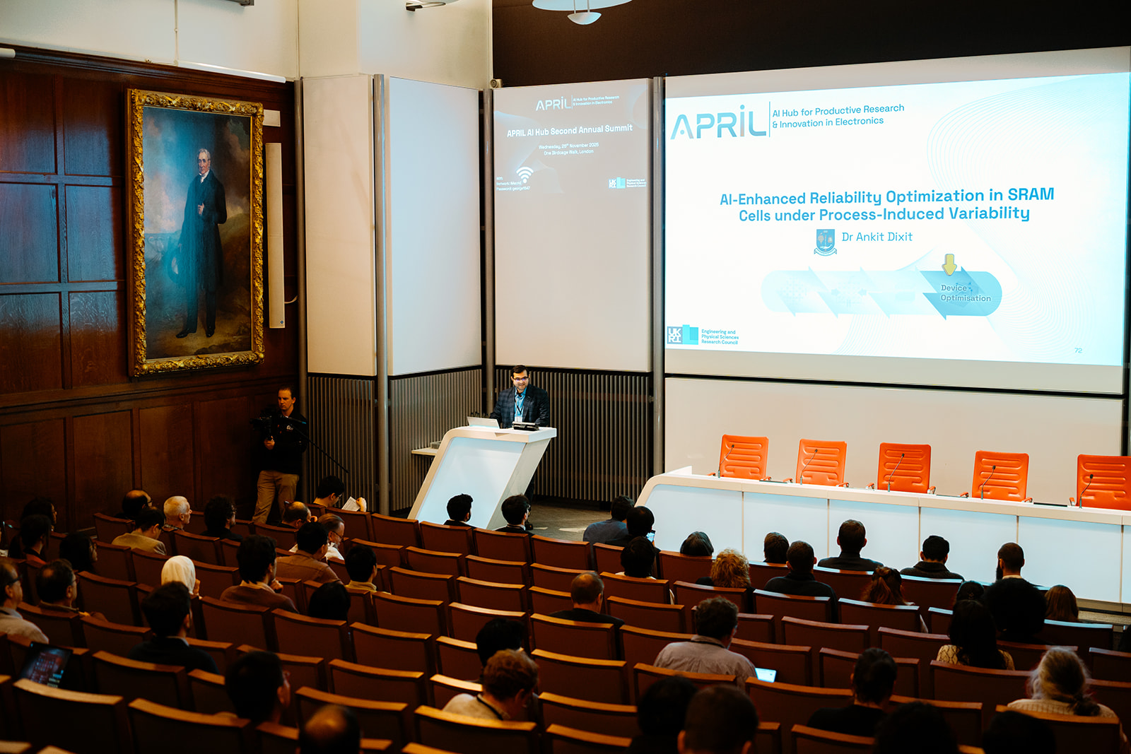
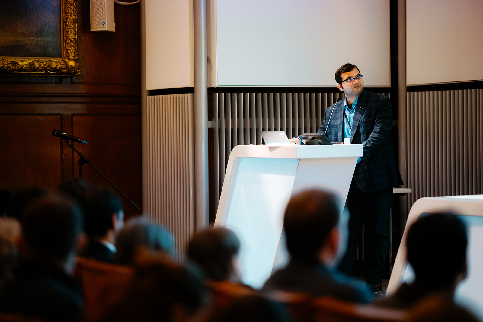
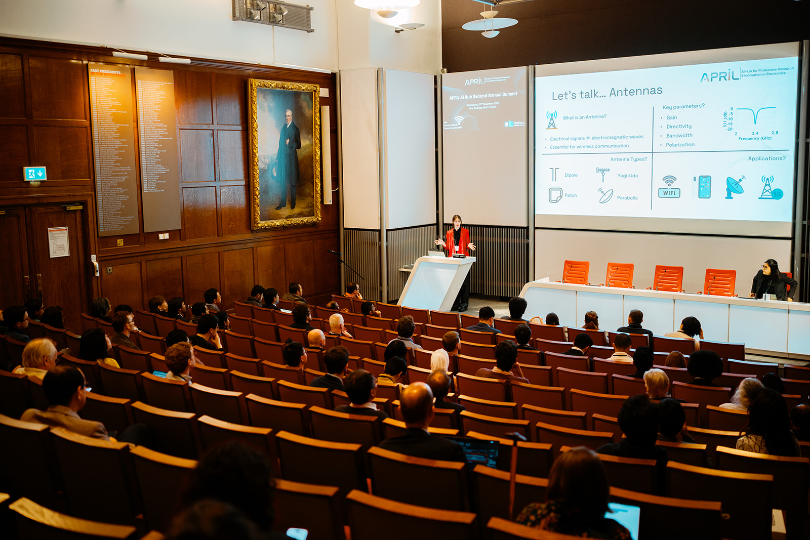
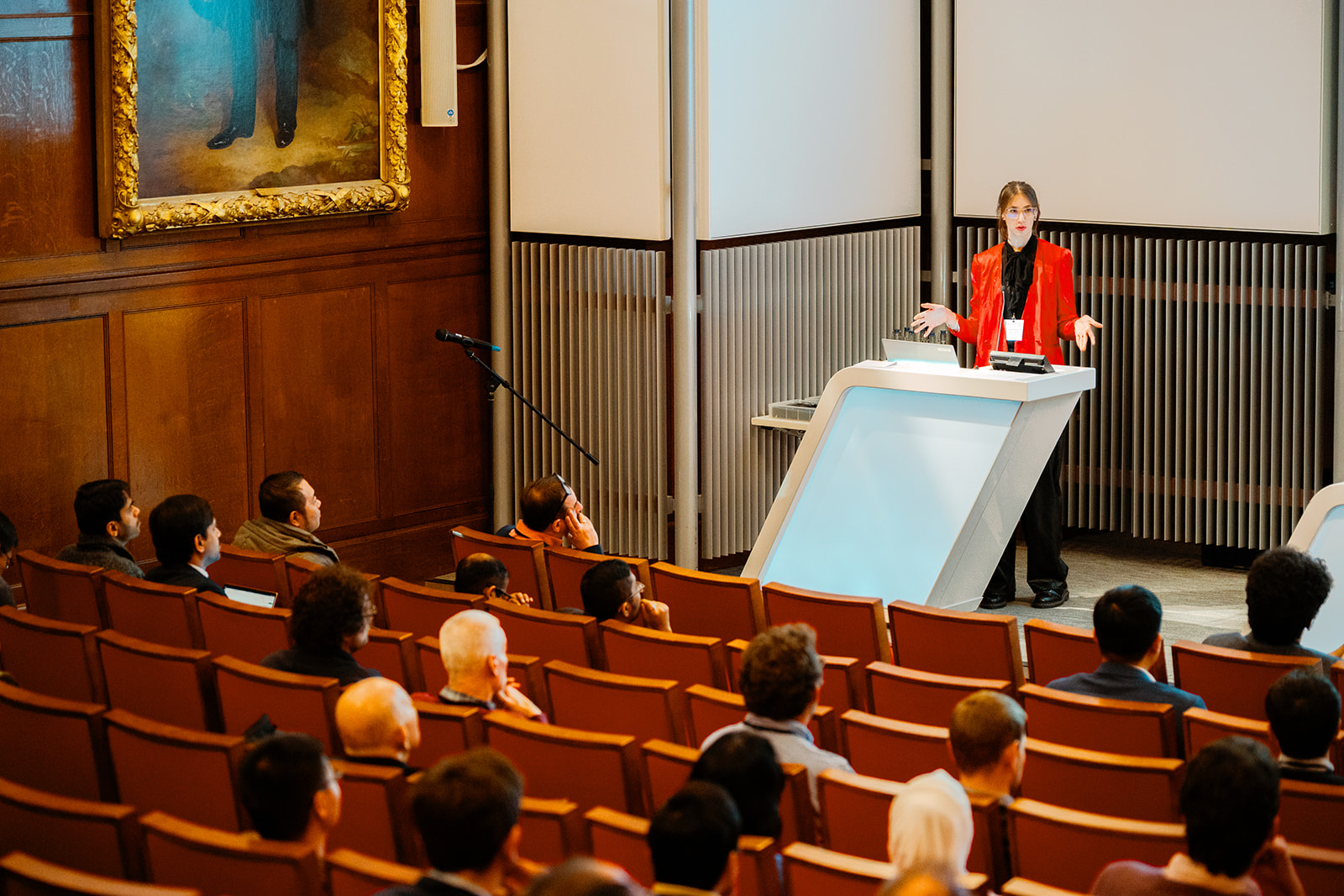
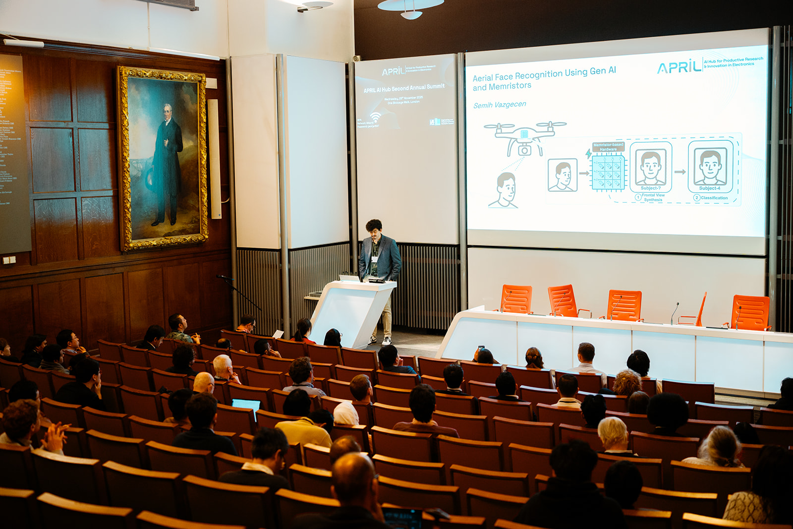
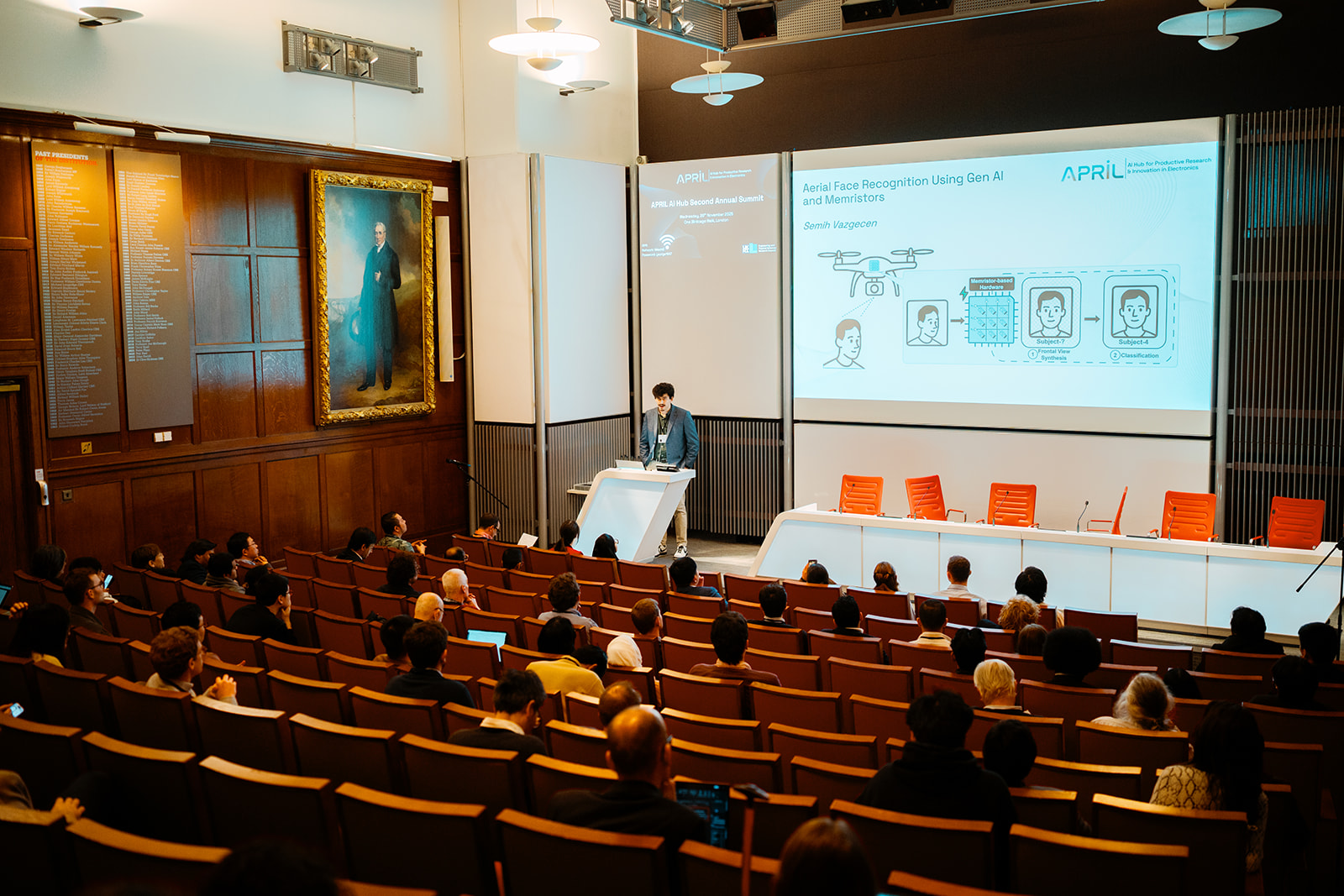
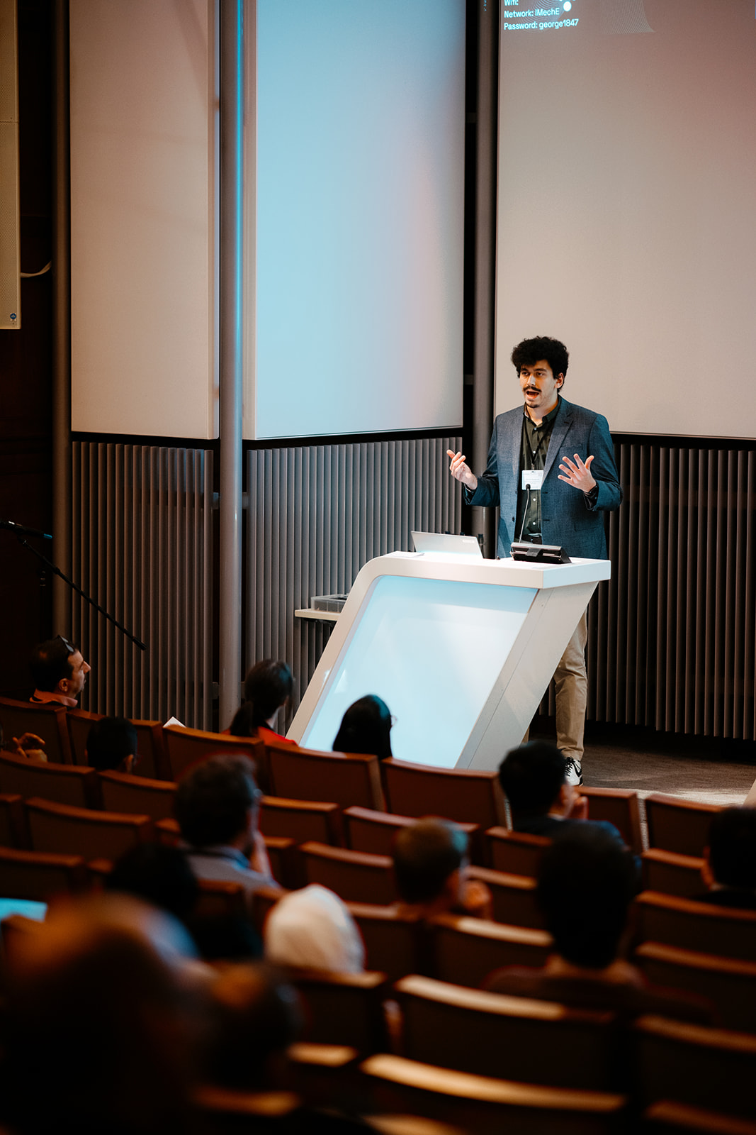
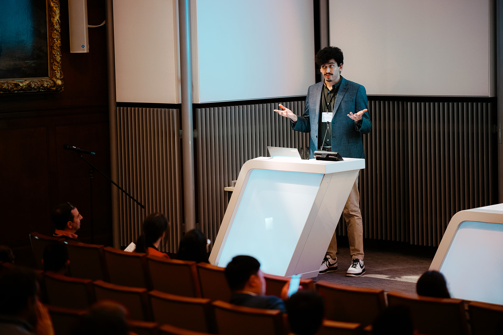
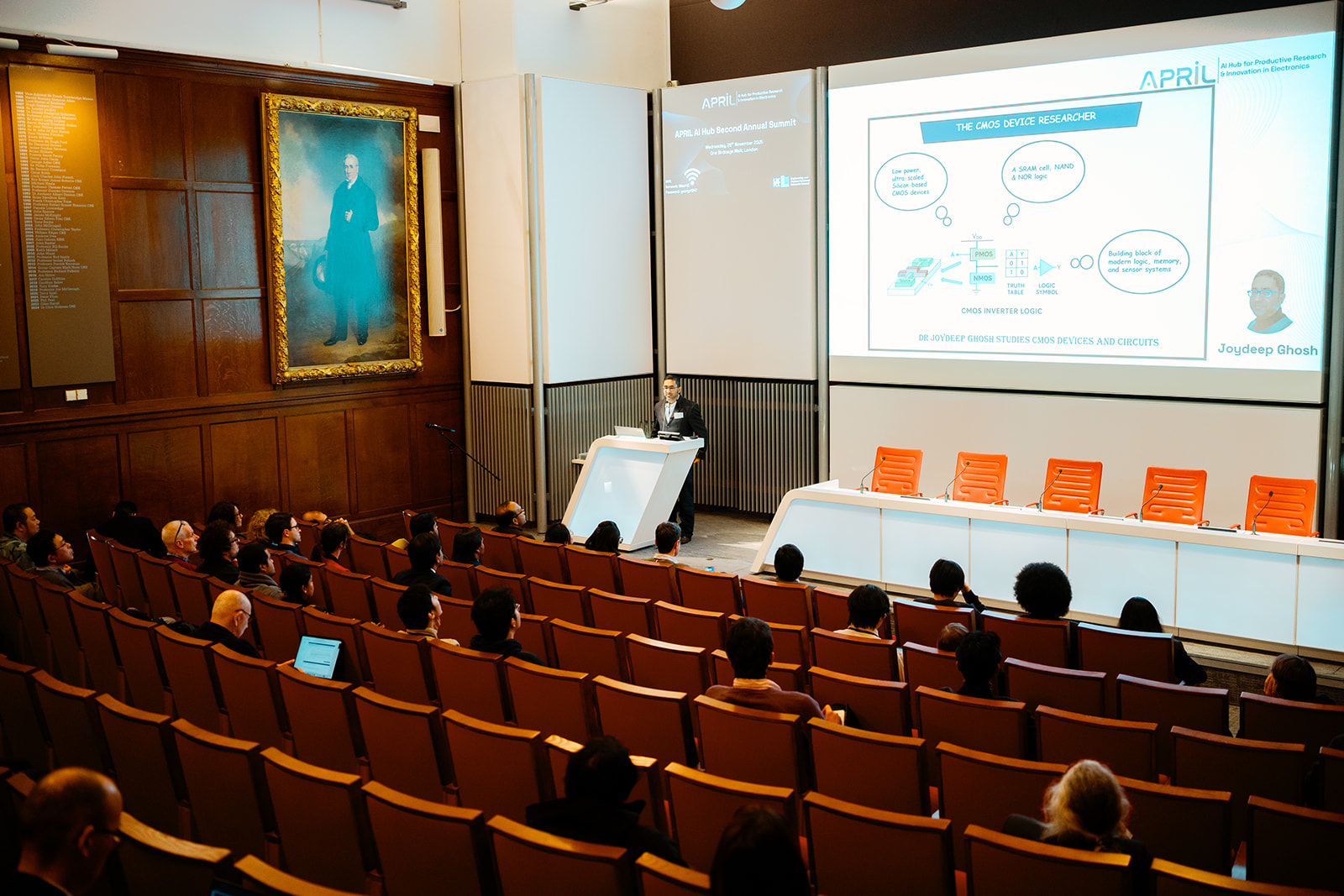
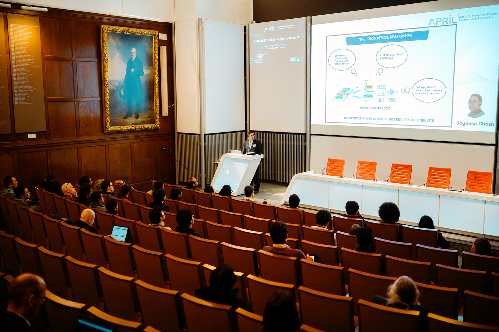
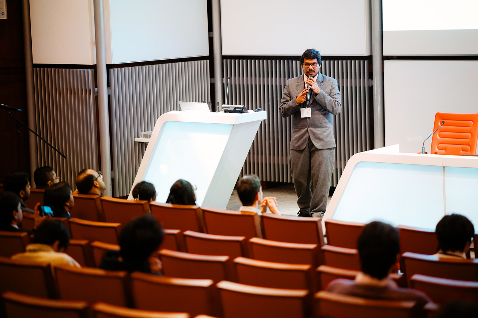
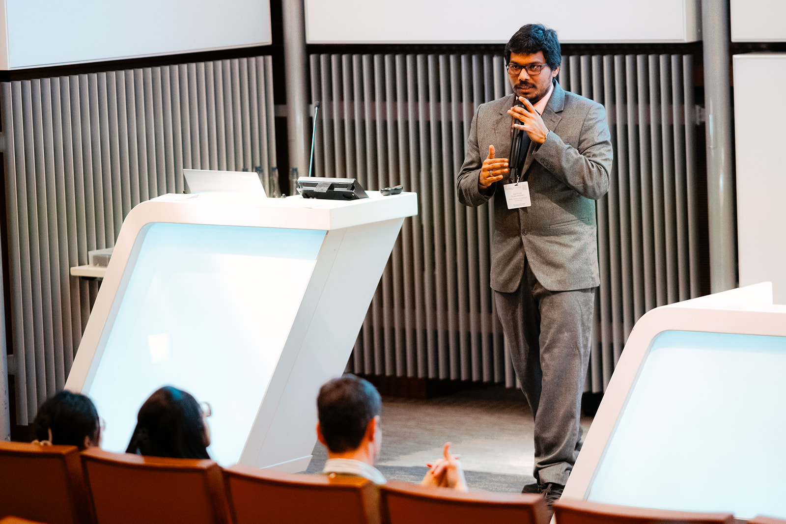
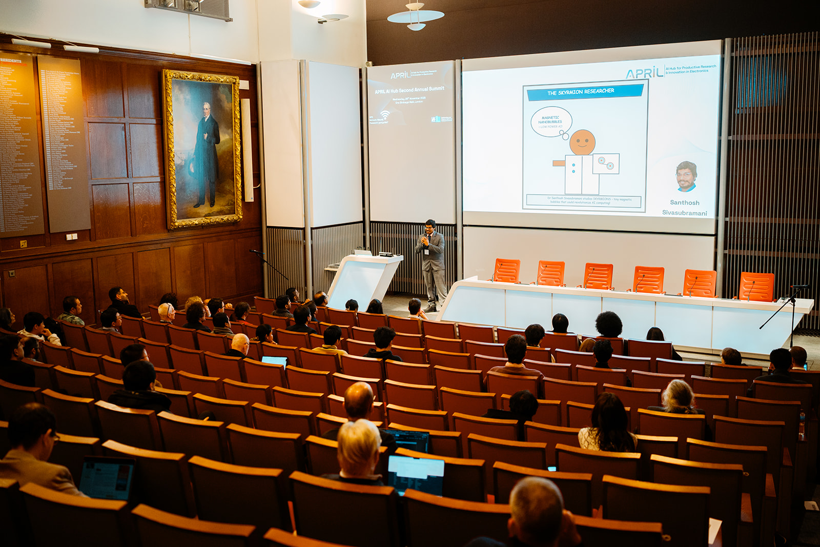
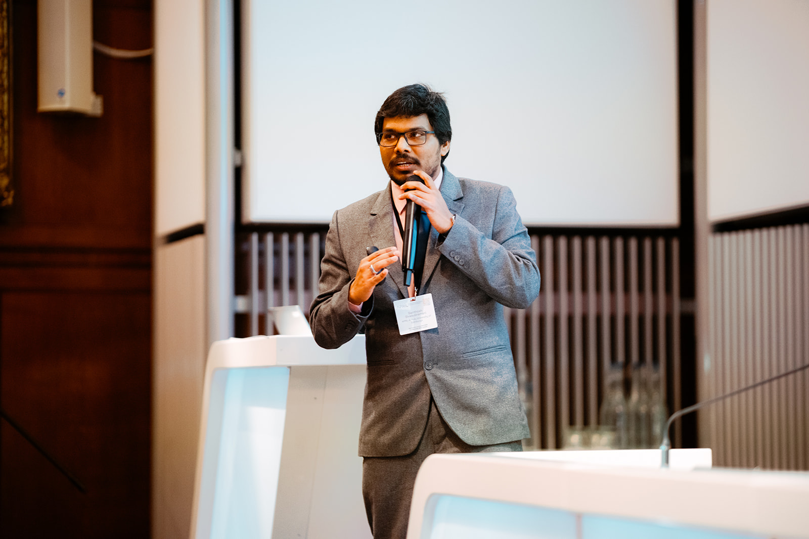
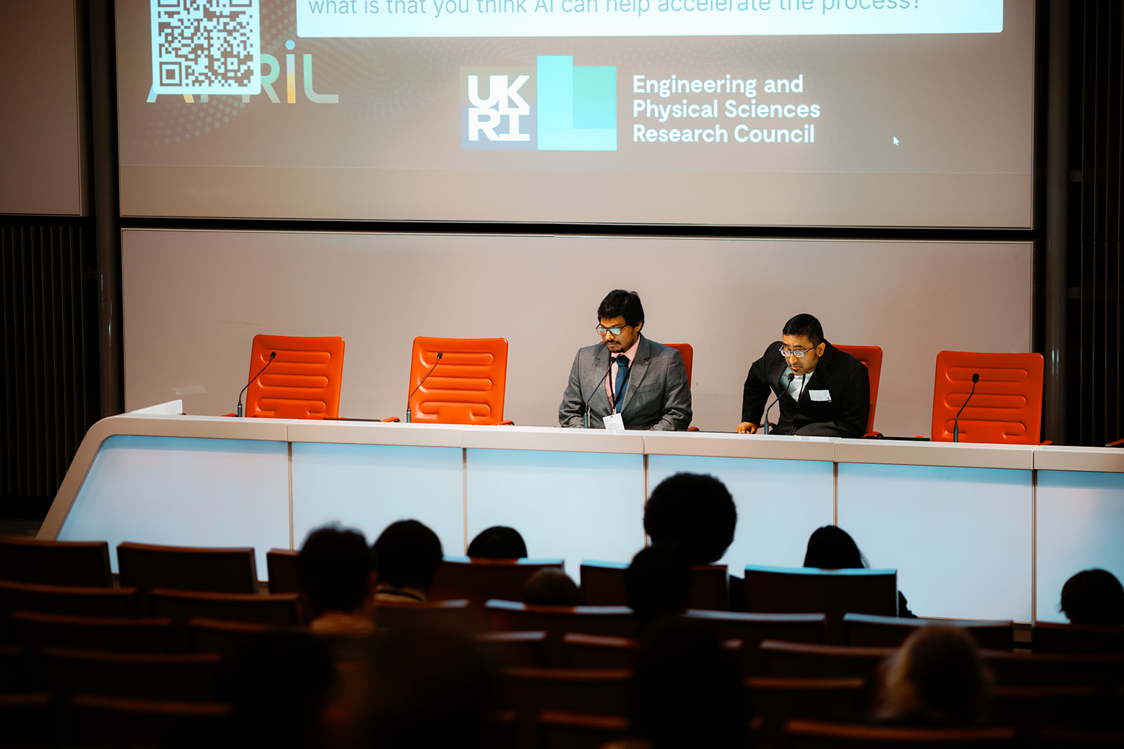
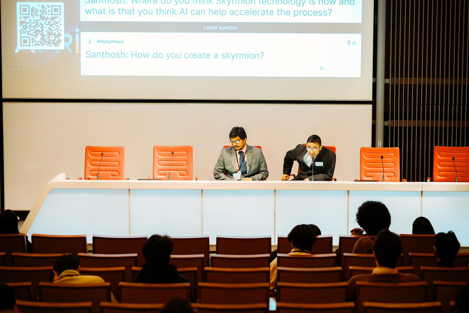
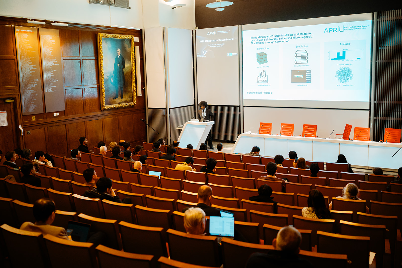
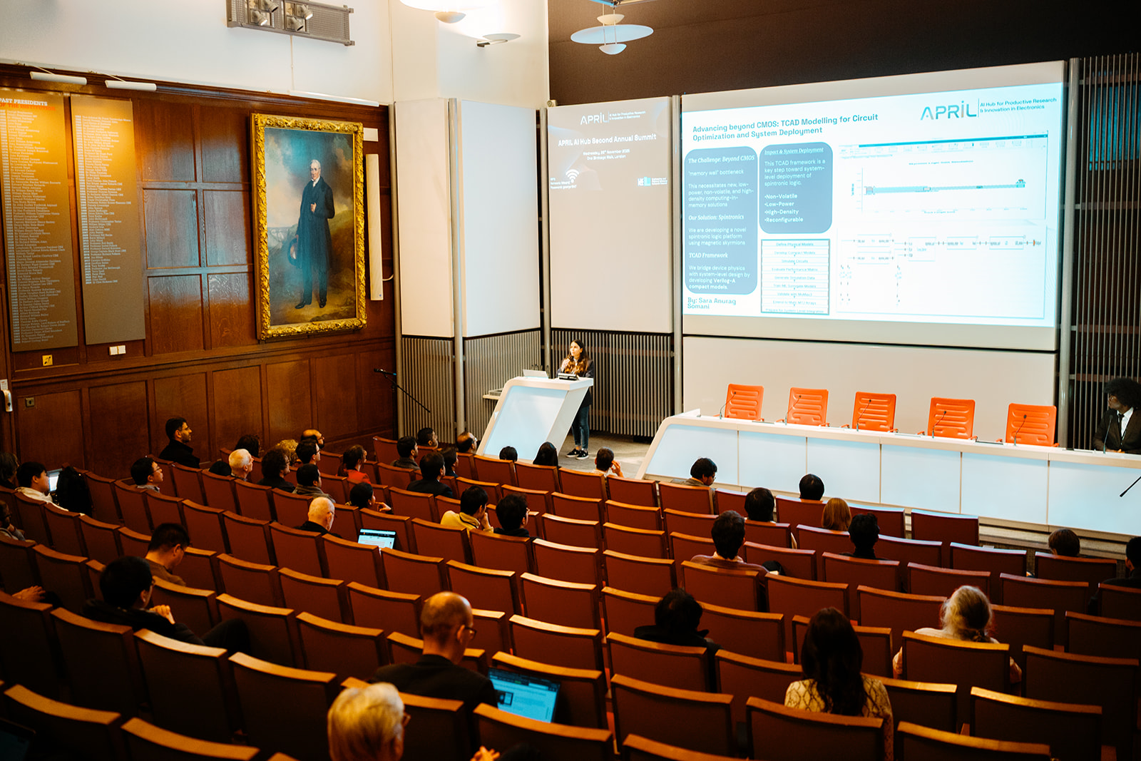
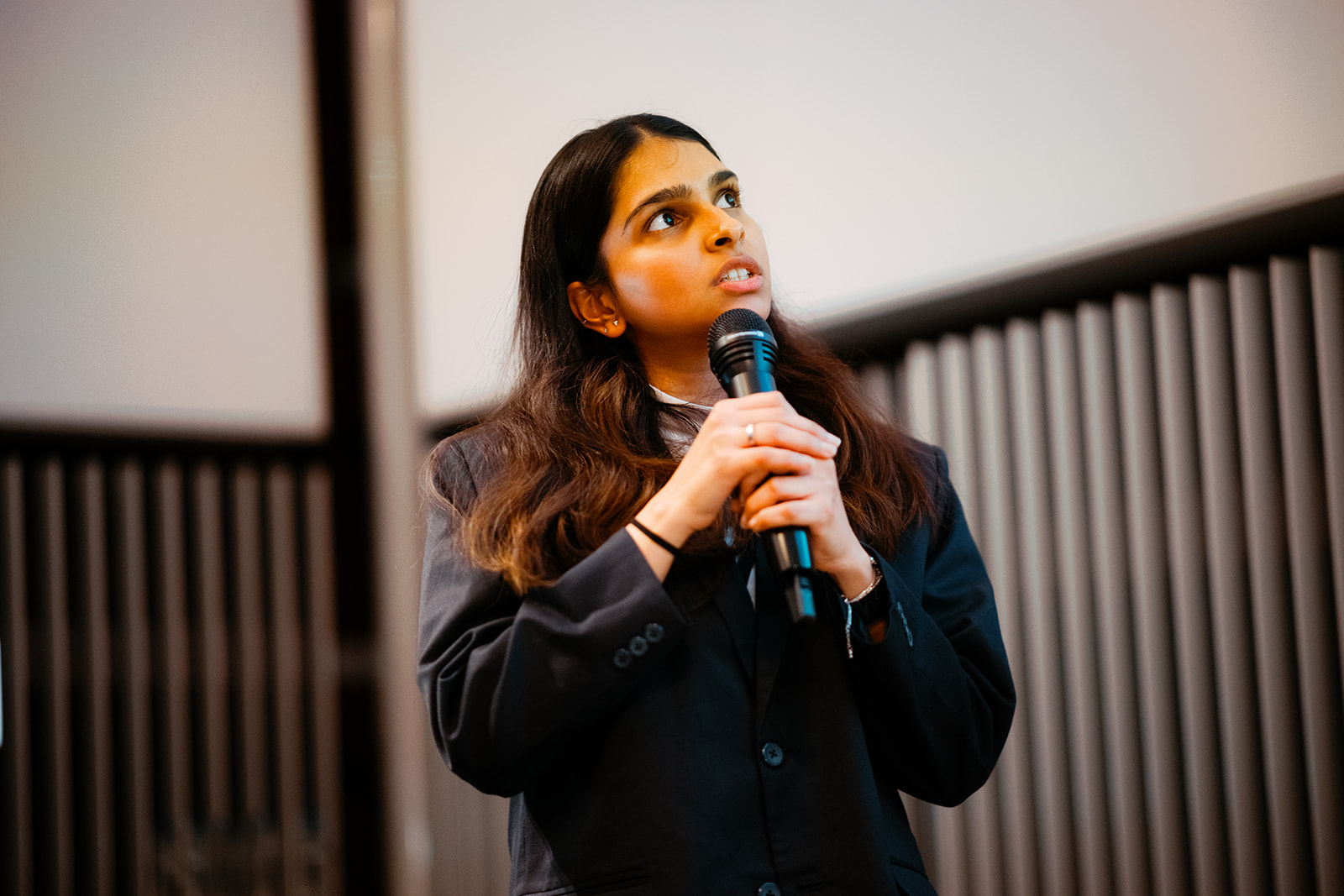
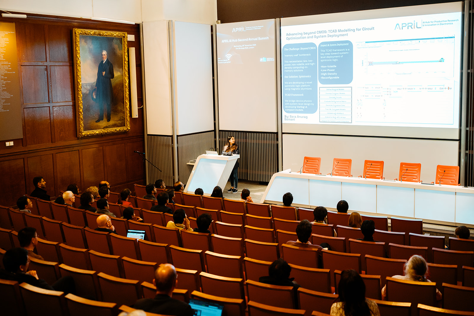
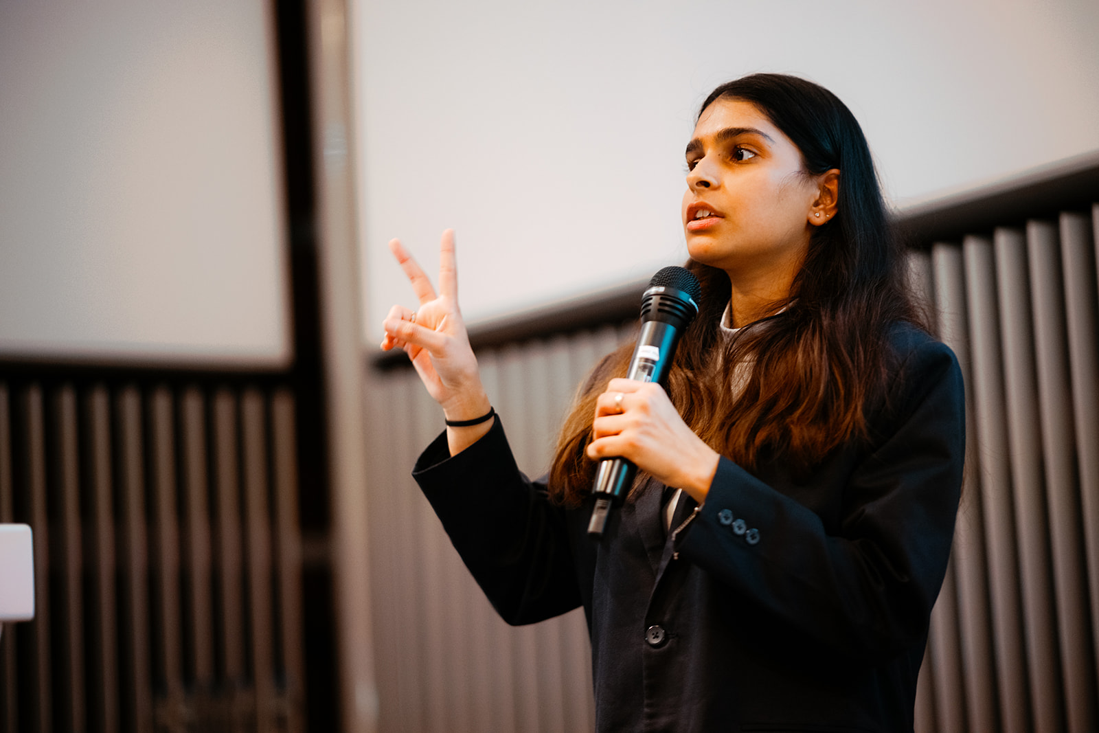
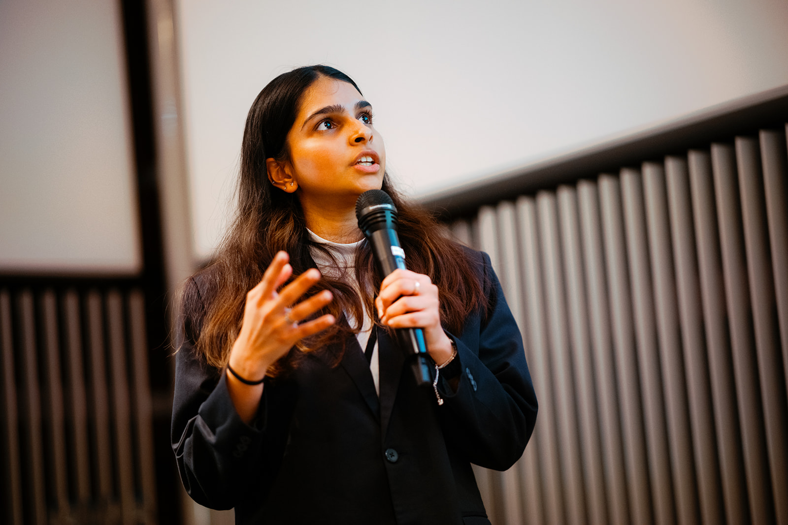
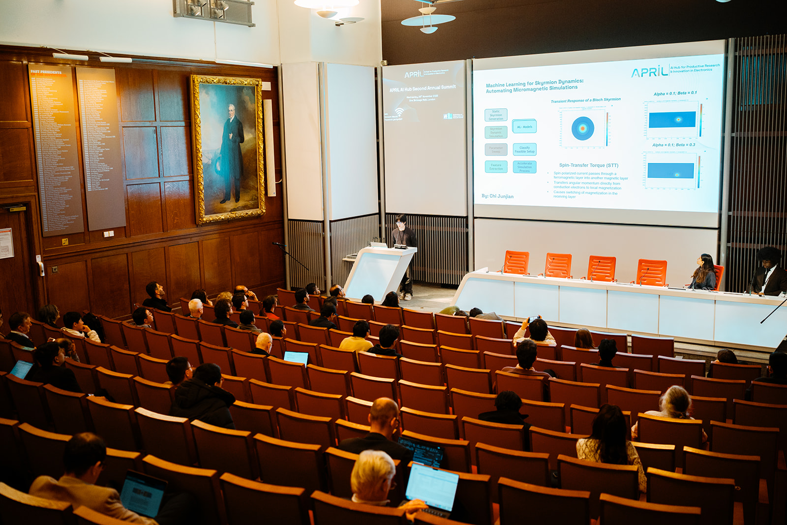
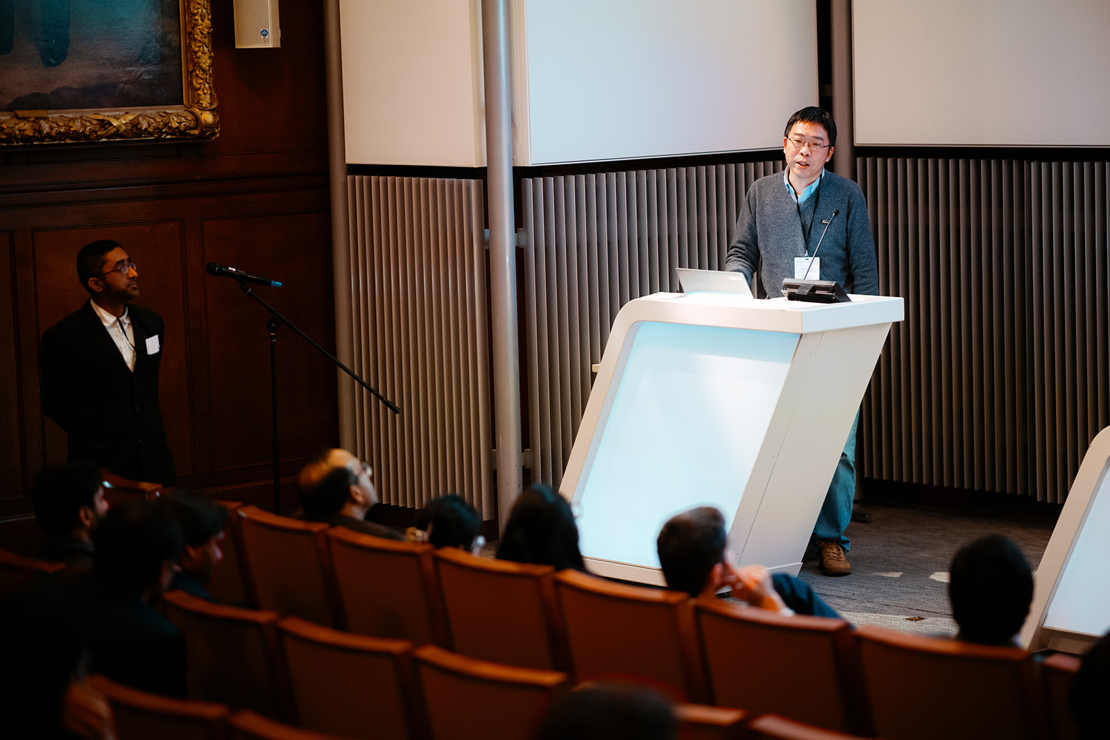
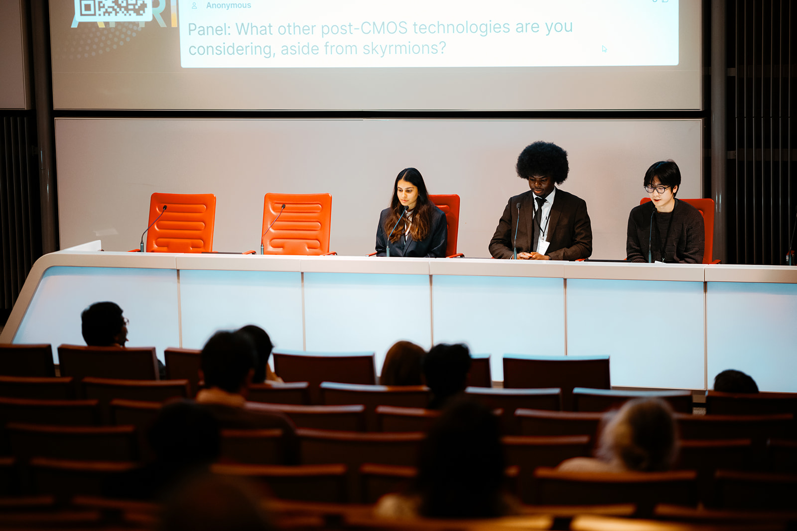
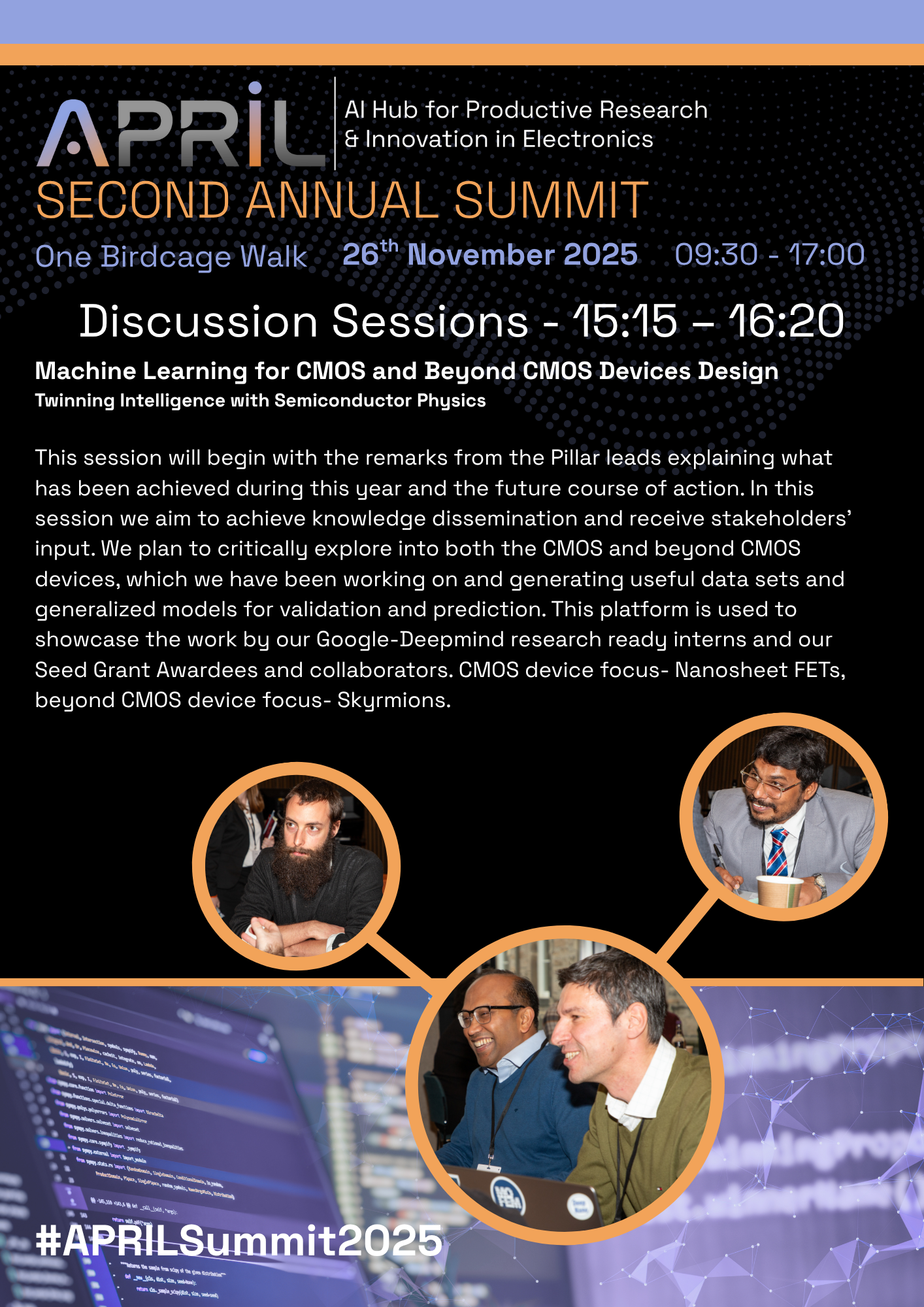
Machine Learning for CMOS and Beyond CMOS Devices Design - 15:15 – 16:20
Twinning Intelligence with Semiconductor Physics
This session will begin with the remarks from the Pillar leads explaining what has been achieved during this year and the future course of action. In this session we aim to achieve knowledge dissemination and receive stakeholders’ input. We plan to critically explore into both the CMOS and beyond CMOS devices, which we have been working on and generating useful data sets and generalized models for validation and prediction. This platform is used to showcase the work by our Google-Deepmind research ready interns and our Seed Grant Awardees and collaborators. CMOS device focus- Nanosheet FETs, beyond CMOS device focus- Skyrmions.